Описание
Характеристики
Заявки просим присылать на адрес sales@texenergo.com
По всем другим вопрос ЦПК support@texenergo.com
ООО «Тэксэнерго Электрик» находится по адресу 141580, Московская обл, Солнечногорский р-н, дер. Черная Грязь, дом 65
Одним из эффективных методов повышения энергоэффективности системы освещения и снижения затрат на её эксплуатацию является использование систем управления освещением. Основываясь на многолетнем опыте эксплуатации различных объектов, холдинг БЛ ГРУПП разработал собственную систему управления АСУНО «БРИЗ».
АСУНО «БРИЗ» включает в себя линейку различного оборудования и ПО, предназначенного для автоматизации систем уличного, архитектурного и промышленного освещения.
— Шкафы управления освещением (ШУНО);
— Регуляторы напряжения;
— Автоматизированные пункты питания наружного освещения (АППНО);
— Контроллеры;
— Программное обеспечение.
Дополнительно НПО GALAD предоставляет услуги по проектированию объектов, шеф-монтажу и обучению персонала клиента. Ниже представлен перечень стандартного оборудования. При этом наша компания предлагает возможность разработки и изготовления оборудования по требованию клиента.
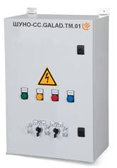
Шкафы управления освещением (ШУНО)
Предназначены для автономного и/или удаленного включения освещения, сбора и обработки диагностической и контрольной информации, коммерческого учета электроэнергии.
Шкаф управления освещением на базе контроллеров БРИЗ-РВ предназначен для автономного включения и отключения наружного освещения по астрономическому расписанию с возможностью синхронизации по системам ГЛОНАСС/GPS. Встроенное программное обеспечение позволяет определять время включения и отключения по координатам установки оборудования (широте и долготе).
Шкаф управления освещением на базе контроллера БРИЗ-ТМ (до 6 отходящих трехфазных линий, связь по GSM/GPRS или Ethernet) предназначен для дистанционного включения и отключения наружного освещения по командам диспетчера, сбора и передачи диагностической информации.
Шкаф управления освещением на базе контроллера БРИЗ DMX. Предназначен для управления архитектурным RGBW освещением по протоколу DMX 512.
Преимущества использования ШУНО:
— Снижение затрат на обслуживание системы освещения за счет удаленного контроля её параметров;
— Точный учет и анализ потребляемой электроэнергии;
— Быстрое выявление и, как следствие, быстрое устранение аварийных ситуаций.
Регуляторы напряжения
Предназначены для группового управления световым потоком в линии методом снижения напряжения в сети. Являются энергосберегающим оборудованием и предназначены для управления процессом пуска, стабилизации и понижения энергопотребления светильников наружного освещения с лампами высокого давления (натриевыми или ртутными), использующих электромагнитные ПРА, и специальными LED светильниками GALAD (LED, Стандарт LED, Волна LED[e6] )
Регулятор напряжения БРИЗ.GALAD
Регулятор напряжения с ручным управлением предназначен для оптимизации расхода электрической энергии, питающей осветительные системы, путем снижения напряжения питания.
Регулятор напряжения БРИЗ.GALAD.РВ
Регулятор напряжения с автоматическим управлением по годовому расписанию предназначен для оптимизации расхода электрической энергии, питающей осветительные системы, путем снижения напряжения питания.
Преимущества использования Регулятора напряжения:
— Экономия потребляемой электроэнергии до 35%;
— Выравнивание фазного напряжения – увеличение срока службы светотехнического оборудования.
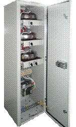
Автоматизированные пункты питания наружного освещения (АППНО)
Предназначены для питания и управления установками наружного освещения по отходящим трехфазным линиям. АППНО выполняет функции вводно-распределительного устройства и имеет возможность подключения регулятора напряжения, а также подсоединение шкафов управления типа ШУНО-СС.GALAD.хх и автоматизированной информационно-измерительной системы учета электроэнергии (АИИСКУЭ).
Автоматизированный пункт питания наружного освещения (6 отходящих трехфазных линий по 100А), обеспечивающий автономное управление наружным освещением с помощью контроллера «БРИЗ-РВ» (автономное включение и отключение наружного освещения по годовому расписанию).
Автоматизированный пункт питания наружного освещения (6 отходящих трехфазных линий по 100А), обеспечивающий дистанционное управление наружным освещением с помощью контроллера «БРИЗ-ТМ» (включение и отключение наружного освещения по командам диспетчера, сбор и передача диагностической информации).
Преимущества использования АППНО:
— Одновременное выполнение функций вводно-распределительного устройства и шкафа управления;
— Полный удаленный контроль системы.
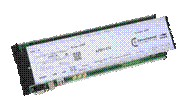
Контроллеры
НПО GALAD предлагает различные контроллеры для автоматизации инфраструктурных сетей и процессов (освещение, водоснабжение, отопление и др.). Все контроллеры являются собственной разработкой компании. Данные контроллеры являются основным компонентом ШУНО, АППНО и регуляторов напряжения.
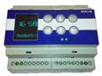
Контроллер управления Бриз РВ
Предназначен для автономного управления наружным освещением по хранящемуся в нем астрономическому расписанию включений и выключений. Имеет в своем составе модуль Глонасс/GPS.
Контроллер управления «БРИЗ-ТМ»
Предназначен для дистанционного включения и отключения наружного освещения по командам диспетчера, сбора и передачи диагностической информации (до 6 отходящих трехфазных линий, связь по GSM/GPRS или Ethernet).
Контроллер управления Бриз-DMX
Предназначен для воспроизведения загруженных цветодинамических сценариев (потоков DMX-512).
Контроллер предназначен для управления уличным освещением по данным календаря, хранящегося в энергонезависимой памяти и показаний часов реального времени. Контроллер имеет два канала управления. Первый канал работает по программе управления (календарю), где указывается время включения и отключения на каждый день года. Второй канал может работать как по календарю, так и в режиме «ночного сокращения освещения».
Общие технические характеристики
Рабочие условия применения:
Относительная влажность от 5 до 95% при 35 °C
Атмосферное давление от 66,0 до 106,7 кПа
Синусоидальные вибрации частотой 10-55 Гц, с амплитудой смещения не более 0,15 мм
Температура транспортирования от минус 40 до плюс 55 °C
Средний срок службы 40 лет
Средняя наработка на отказ 140 000 часов
Основные технические и метрологические характеристики:
Номинальное напряжение питания 220 (+10/-15) В
Потребляемая мощность 6 Вт
Количество каналов управления 2
Коммутируемое напряжение не более 250 В
Коммутируемый ток на канал не более 0,3 А
Количество срабатываний 1 000 000
Тип батареи CR 2032
Ведение времени при отсутствии питания 1 год
Срок хранения батареи 10 лет
Погрешность хода часов 1 сек/сутки
Сеть SyBus
Физический интерфейс сети RS-485
Скорость обмена 9600, 38400, 153600, 307200 бод
Степень защиты IP20
Диапазон рабочих температур окружающего воздуха от -40 до +70 °C
Масса 0,6 кг
На чтение 20 мин Просмотров 6 Опубликовано 11 апреля 2023 Обновлено 11 апреля 2023
Содержание
- Основные виды схем управления освещением
- Управление освещением при помощи автоматических выключателей в щите
- Управление освещением местными выключателями с одного, двух, трех и более мест
- Управление выключателями с одного места
- Управление выключателями двух мест
- Управление выключателями трех и более мест
- Управление освещением с использованием импульсного реле
- Управление освещением с использованием контакторов (магнитных пускателей)
- Конструкция контактора и принцип работы
- Базовая схема управления освещением при помощи контактора
- Схемы управления освещением при помощи контактора и кнопок — схема «самоподхвата»
- Базовая схема и принцип работы
- Схема «самоподхвата» для управления освещением с нескольких мест
- Схемы управления освещением при помощи контактора и импульсного реле
- Управление освещением с использованием реле времени
- Базовая схема и принцип работы
- Схемы управления освещением нескольких линий при помощи реле времени
- Управление освещением с использованием реле времени для лестничных клеток
- Управление освещением с использованием фотореле
- Управление освещением с использованием реле напряжения
- Управление освещением с использованием датчиков движения
- Управление освещением с использованием контроллеров
- Скачать примеры схем управления освещением
Основные виды схем управления освещением

В статье рассмотрим основные виды схем управления освещением, которые применяются в щитах освещения и шкафах управления освещением как для автоматического, так и для ручного управления наружным (уличным, декоративным) и внутренним освещением.
Управление освещением при помощи автоматических выключателей в щите
Простейшим способом управления освещением является включение и отключение автоматического выключателя в щите освещения. Это решение применяется в щитах аварийного освещения с постоянно горящими светильниками, которые не требуют частого включения и отключения, а доступ к управлению освещением должен иметь только квалифицированный персонал.
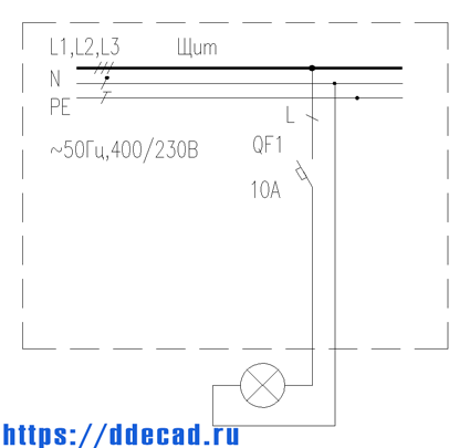
Схема управления освещением при помощи автомата в щите
Но вообще, автоматические выключатели не предназначены для частого включения и отключения, поэтому для управления освещением дополнительно внутрь щита устанавливают выключатель.
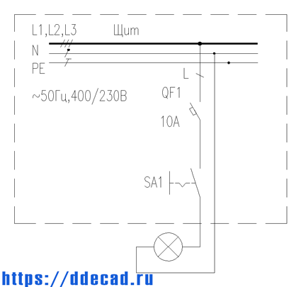
Схема управления освещением при помощи переключателя внутри щита
У ведущих производителей подобные выключатели есть в модульном исполнении (например, переключатели E211 у ABB или iSSW у Schneider Electric).
Номинальный ток переключателя ограничен, поэтому для управления мощными нагрузками его может быть недостаточно. В таком случае следует использовать схемы управления освещением при помощи контакторов.
Управление освещением местными выключателями с одного, двух, трех и более мест
Самый распространённый способ управления освещением — выключателями освещения. Данный способ знаком каждому, т.к. управление освещением в квартирах реализовано именно так. Этот способ применяется также в общественных (офисные, торговые, административные) и промышленных зданиях для местного управления освещением.
Управление выключателями с одного места
Простейший и наиболее распространённый — управлением одно- , двух- и трехклавишными выключателями с одного места.
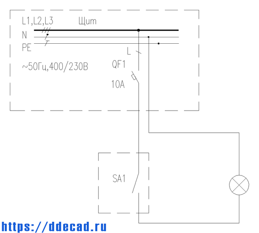
Схема управления освещением одноклавишным выключателем
Двухклавишные и трехклавишные выключатели позволяют управлять несколькими светильниками или разными группами включения в многоламповом светильнике.
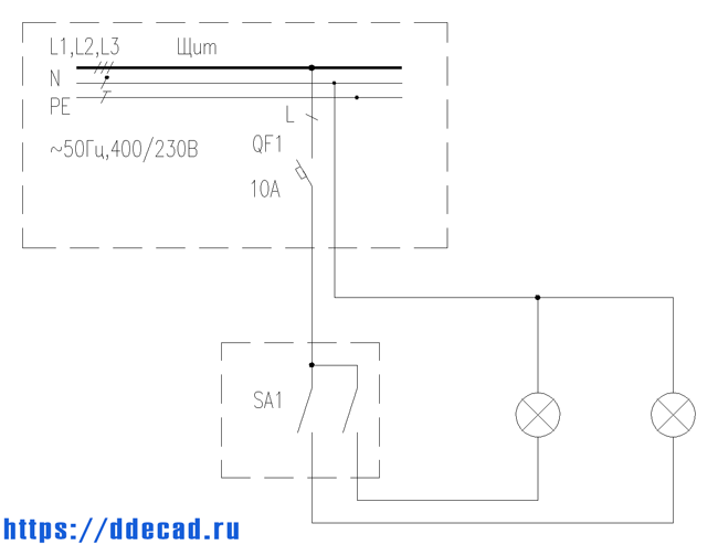
Схема управления освещением двухклавишным выключателем
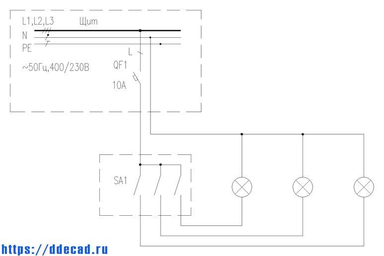
Схема управления освещением трехклавишным выключателем
Управление выключателями двух мест
Для управления освещением в двух мест используют переключатели. Внешне они выглядят как обычные выключатели, но конструктивно отличаются. Такой переключатель содержит перекидной контакт. Соответственно, включение и отключение светильника зависит от положения клавиш на обоих переключателях.

Схема управления освещением переключателями с двух мест
Данная схема управления чаще всего используется в коридорах, т.к. позволяет включить освещение при входе в коридор и отключить при выходе из него. Также переключатели используют для управления освещением в гостиничных номерах и квартирах. Удобно включить общее освещение при входе в спальню, а отключить не вставая с кровати.
Управление выключателями трех и более мест
Для управления освещением с трех мест потребуется ещё один вид выключателя — перекрестный переключатель. Он устанавливается в схеме между переключателями (на схеме обозначен SA2).

Схема управления освещением переключателями с трех мест
Для управления освещением с четырёх мест потребуется установка ещё одного перекрестного переключателя.

Схема управления освещением переключателями с четырех мест
Теоретически, таким образом можно организовать управлением освещением с большого числа мест, добавляя в схему перекрестные переключатели, но так не делают. С точки зрения простоты схемы, удобства и по экономическим соображениям, управление с трех и более мест целесообразнее делать с использованием импульсных реле и кнопочных выключателей.
Управление освещением с использованием импульсного реле
Импульсное реле позволяет организовать управление освещением одного, двух, трех, четырех и практически неограниченного числа мест. Для реализации схемы потребуется импульсное (бистабильное) реле и кнопочные (нажимные) выключатели.
Для понимания логики работы схемы следует разобраться с особенностями работы импульсного реле. Это реле каждый раз переключает свои контакты при подачи импульса на катушку управления.
В зависимости от производителя, подача импульса может быть как на основной питающий вход реле, так и на отдельный вход управления.
Существуют различные версии импульсного реле с разным набором пар контактов NO (нормально открытыми), NC (нормально закрытыми), перекидными контактами и их различной комбинацией.
Рассмотрим работу схемы управления освещением с самой простой версией импульсного реле с одной NO парой контактов.

Схема управления освещением при помощи импульсного реле
Силовая цепь питания светильников состоит из автоматического выключателя QF1 и контактов импульсного реле KI1. Управление импульсным реле осуществляется кнопочными (нажимными) выключателями SB1, SB2. подключенными параллельно на клеммы X1:1 и X1:2.
В начальном положении контакты реле KI1 разомкнуты (NO). При нажатии на кнопку SB её контакты 1 и 2 замыкаются и на катушку реле поступает управляющий импульс. Реле меняет положение контактов — силовая цепь замыкается, освещение включается.
Повторное нажатии на кнопку SB подаст на катушку реле ещё один импульс и реле опять сменит состояние контактов — силовая цепь разомкнётся, освещение отключится.
Как видим, применяя данную схему можно существенно сэкономить на кабеле и монтажных работах.
Схемы с использованием импульсного реле для управления освещением применяют в жилых, общественных и промышленных зданиях.
Управление освещением с использованием контакторов (магнитных пускателей)
Контакторы (магнитные) пускатели широко используются в схемах управления освещением и инженерным оборудованием.
Конструкция контактора и принцип работы
Конструктивно контактор состоит из неподвижной части сердечника, катушки, неподвижной группы контактов, подвижного сердечника с подвижной парой контактов.
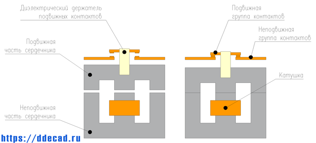
При подачи напряжения на катушку, подвижная часть сердечника под воздействием электромагнитного поля вместе с закреплённой на ней подвижной группой контактов притягивается к неподвижной части сердечника. При этом подвижная и неподвижная группа контактов замыкается.
При снятии напряжения с катушки, подвижная часть сердечника под воздействием пружины возвращается в исходное положение и группы контактов размыкаются.
Мы рассмотрели принцип работы контактора с NO (нормально разомкнутыми) контактами. Аналогичным образом работают контакторы с NC (нормально закрытыми) контактами и перекидными контактами.
Базовая схема управления освещением при помощи контактора
Рассмотрим работу базовой схемы управления освещением при помощи контактора. Силовая цепь питания светильников состоит из автоматического выключателя QF1 и NO (нормально открытых) контактов контактора KM1. Цепь управления состоит из автоматического выключателя SF1 и катушки контактора KM1, между которыми включается контакт управляющего элемента (подключается между клеммами X1:1 и X1:2).
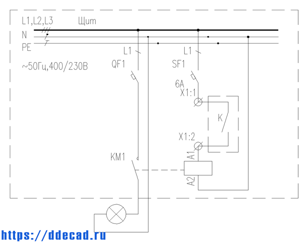
Управление освещением при помощи контактора. Базовая схема
Управляющий контакт K разомкнут, катушка контактора KM1 без напряжения, контакты контактора разомкнуты.
При замыкании управляющего контакта K на катушку контактора KM1 подаётся питание и контактор замыкает свои контакты. Силовая цепь замкнута — освещение включается.
При размыкании управляющего контакта цепь управления размыкается. С катушки контактора снимается напряжение и его контакты возвращаются в исходное положение (разомкнуты). Силовая цепь размыкается — освещение отключается.
В качестве управляющего контакта может выступать обычный одноклавишный выключатель освещения, устанавливаемый в нужном месте на стене помещения. Такая схема применяется в квартирах, когда устанавливают при входе в квартиру мастер-выключатель, отключающий все нагрузки кроме тех, которые нельзя отключать (холодильник, например).
Такая же схема с мастер-выключателем применяется в гостиницах, когда в щите номера устанавливают контактор, управляемый карточным выключателем.
Также в качестве управляющего выключателя может выступать выключатель или переключатель SA1, устанавливаемый в щите (например, модульный переключатель E211 у ABB, iSSW у Schneider Electric или подобный).
Управление освещением при помощи контактора и выключателя в щите
Схемы управления освещением при помощи контактора и кнопок — схема «самоподхвата»
Часто при управлении освещением производственных зданий, а также наружного освещения применяется схема «самоподхвата».
Базовая схема и принцип работы
Рассмотрим работу схемы для питания однофазной цепи освещения. Для реализации данной схемы нам понадобятся:
- автоматических выключателя QF1 для защиты силовой цепи
- автоматический выключатель SF1 для защиты цепи управления
- контактор KM1 c двумя парами нормально разомкнутых контактов 2NO
- кнопка SB1 «ПУСК» с нормально разомкнутыми контактами NO
- кнопка SB2 «СТОП» с нормально замкнутыми контактами NC
- сигнальная лампа HL1 для индикации включения освещения

Управление освещением при помощи контактора и кнопок — схема самоподхвата
Кнопки SB2, SB1 и катушку контактора KM1 подключаем последовательно друг за другом. Параллельно с катушкой подключаем сигнальную лампу. Первую пару NO контактов контактора KM1.1 подключаем в силовую цепь, а вторую пару NO контактов контактора KM1.2 подкючаем параллельно NO контактам кнопки SB1.
- В начальном положении цепь управления разомкнута: контакты кнопки SB1 разомкнуты, катушка контактора KM1 без напряжения, пары контактов KM1.1 и KM1.2 разомкнуты, лампа HL1 не горит.
- Нажимаем кнопку SB1. Контакты SB1 замыкаются, контакты SB2 замкнуты, на катушку контактора KM1 подаётся напряжение и загорается сигнальная лампа HL1. Контактор KM1 замыкает свои пары контактов KM1.1 и KM1.2. Силовая цепь замыкается и включается освещение.
- Отпускаем кнопку SB1. Контакты SB1 размыкаются, но подключенная параллельно пара контактов KM1.2 замкнута, поэтому катушка контактора KM1 остаётся под напряжением и не размыкает свои пары контактов.
- Нажимаем кнопку SB2. Контакты SB2 размыкаются, с катушки контактора KM1 снимается напряжение, пары контактов KM1.1 и KM1.2 размыкаются, сигнальная лампа гаснет, освещение отключается.
Как видим, при замыкании кнопки SB1 контактор сам «подхватывает» своё питание за счёт второй пары контактов. Из-за этого данную схему назвали схемой «самоподхвата».
Пожалуй, это одна из основных схем для шкафов и пультов управления освещением. Корпус шкафа делают металлическим, а на переднюю дверцу выводят кнопки и сигнальные лампы. Эту же схему применяют для управления двигателями.
Схема «самоподхвата» для управления освещением с нескольких мест
Также схему «самоподхвата» можно применить для управления освещением с нескольких мест. В этом случае в качестве пар кнопок использую кнопочные посты, устанавливаемые в нужных местах.
Нормально открытые NO контакты кнопочных постов соединяем параллельно, нормально закрытые NC контакты — последовательно. Таким образом, замыкание любого NO-контакта замкнёт цепь питания катушки контактора, а размыкание любого NC-контакта разомкнёт.

Управление освещением с нескольких мест при помощи контактора и кнопок — схема самоподхвата
Подобным образом можно управлять сразу несколькими группами освещения одновременно. Для этого нужно немного видоизменить схему. Контактор 4KM1, установленный в цепи управления, одной парой контактов 4KM1.2 будет «подхватывать» своё питание, а второй парой контактов 4KM1.1 управлять питанием катушек контакторов, включающих освещение.

Управление освещением нескольких групп с нескольких мест при помощи контактора и кнопок — схема самоподхвата
Схемы управления освещением при помощи контактора и импульсного реле
Ещё одним вариантом схемы управления с нескольких мест является комбинированная схема с использованием контакторов и импульсного реле. Данную схему применяют в случае, когда одной кнопкой нужно включить сразу несколько групп освещения.
Рассмотрим данный тип схемы для управления тремя группами освещения с трех мест.
- В начальном состоянии контакты импульсного реле KI1 разомкнуты. Катушки контакторов 1KM1, 2KM1, 3KM1 находятся без напряжения, их пары контактов разомкнуты. Силовые цепи разомкнуты и освещение отключено.
- Нажимаем кнопку, например, SB1и, тем самым, подаем управляющий импульс на катушку импульсного реле KI1. Импульсное реле меняет состояние контактов и замыкает свою пару контактов. На катушки контакторов 1KM1, 2KM1, 3KM1 подаётся напряжение и они замыкают свои пары контактов. Силовые цепи замыкаются и включается освещение.
- Повторно нажимаем кнопку SB1 (либо любую другую — SB2, SB3) и подаем управляющий импульс на катушку импульсного реле KI1. Импульсное реле меняет состояние контактов и размыкает свою пару контактов. Напряжение с катушек контакторов 1KM1, 2KM1, 3KM1 снимается и они размыкают свои пары контактов. Силовые цепи размыкаются и освещение отключается.

Управление освещением нескольких групп с нескольких мест при помощи контактора и импульсного реле
При необходимости, данную схему можно доработать, включив параллельно катушкам контакторов сигнальную лампу, а также установить в щите кнопку для включения освещения с дверцы щита.
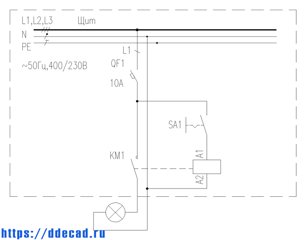
Управление освещением с использованием реле времени
Реле времени широко используются в схемах автоматики, в том числе для управления освещением.
Реле времени можно разделить на две большие группы:
- Программируемые реле времени — реле замыкает и размыкает свои контакты в соответствии с заданной программой;
- Таймеры — реле времени замыкает размыкает свои контакты на заданное время после приложения управляющего сигнала.
Программируемые реле времени и таймеры могут быть электронными и электромеханическими.
Программируемые реле времени могут быть с суточным (одна и та же программа повторяется каждые сутки), недельным (одна и та же программа повторяется каждую неделю) и годовым циклом (программа задаётся на год).
Базовая схема и принцип работы
Рассмотрим работу схемы управления освещением на базе программируемого реле времени, работающего по одной суточной программе.

Управление освещением при помощи реле времени. Базовая схема
Допустим, освещение должно быть включено ежедневно с 9:00 до 18:00. В реле времени устанавливаем текущее время и задаем программу, в соответствии с которой в 9:00 реле должно замкнуть свои контакты сроком на 9 часов. Ежедневно, при наступлении 9:00 реле времени KT1 замыкает свои контакты, силовая цепь оказывается замкнутой и освещение включено. Через 9 часов работа программы заканчивается и реле размыкает свои контакты — освещение отключается.
Схемы управления освещением нескольких линий при помощи реле времени
Для управления несколькими линиями по одной программе применяют реле времени в комбинации с контакторами. Контакторы включают и отключают питание, а реле времени управляет их работой.

Управление освещением при помощи реле времени и контакторов
Питание на катушки контакторов 1KM1, 2KM1, 3KM1 подаётся через трехпозиционный переключатель SA1 с нейтральным положением:
- В положении «Ручное» питание напрямую подаётся на катушки контакторов KM и они замыкают свои пары контактов, освещение включается в соответствии с заданной программой;
- В положении «0» цепь питания катушек контакторов разорвана и освещение отключено;
- В положении «Автомат» питание на катушки контакторов подаётся через контакты реле времени KT1. Включением и отключением освещения управляет реле времени, замыкая и размыкая свои контакты в соответствии с заданной программой.
При необходимости, можно дополнить схему сигнальной лампой HL, включенной параллельно катушкам контакторов, которая будет информировать о включении освещения.
Управление освещением с использованием реле времени для лестничных клеток
Для экономии электроэнергии и управления освещением с нескольких мест используют реле времени из группы таймеров. Данный тип реле замыкают или размыкают свои контакты после подачи на их катушку управляющего сигнала, замыкание или размыкание контактов происходит с заданной временной задержкой.
Основное применение данный тип реле времени нашёл в схемах управления двигателями и схемах АВР (автоматического ввода резерва), но для управления освещением также используется. Например, для управления освещением лестничных клеток.
Рассмотрим применение и работу реле времени для решения данной задачи:
- В начальный момент времени контакты реле KT1 разомкнуты, освещение отключено. Кнопки SB1, SB2. установлены на каждом этаже лестничной клетки и подключены параллельно к управляющим контактам реле времени KT1.
- При нажатии любую из кнопок SB, на катушку реле времени KT1 поступает управляющий сигнал, оно замыкает свои контакты, освещение включается, а реле времени начинает отсчет.
- По прошествии заданного времени реле KT1 размыкает свои контакты и освещение отключается.
- Если при замкнутых контактах реле (т.е. до истечения заданного времени) поступает новый управляющий сигнал, то отсчет времени начинается заново.

Управление освещением лестничных клеток с использованием реле времени
Таким образом, человек, заходя на лестничную клетку, нажимает кнопочный выключатель SB и включает освещение. На следующем этаже опять нажимает кнопку и т.д. Через заданное время освещение на лестничной клетке отключается. Настройка задержки отключения выбирается таким образом, чтобы человек достаточно времени, чтобы дойти от одного кнопочного выключателя до другого.
Данную схему можно также использовать для управления освещением в коридорах. Она позволяет организовать включение освещения с нескольких мест (как при использовании импульсного реле) и при этом ещё сэкономить электроэнергию.
Управление освещением с использованием фотореле
Фотореле (сумеречное реле, сумеречный выключатель) используют для управления наружным (уличным, декоративным) освещением. Фотореле состоит из двух частей: самого реле, устанавливаемого в щит, и выносного датчика освещенности.
Рассмотрим работу схемы управления наружным освещением на базе самой простой версии фотореле, реагирующей только на уровень освещенности.
Датчик освещенности (фотодатчик) BL1 подаёт сигнал на фотореле KL1 пропорционально уровню освещённости. При снижении уровня освещённости ниже заданного, фотореле KL1 замыкает свою пару контактов. Силовая цепь замыкается, включается наружное освещение. При повышении уровня освещенности выше заданного, фотореле KL1 размыкает свою пару контактов и наружное освещение отключается.
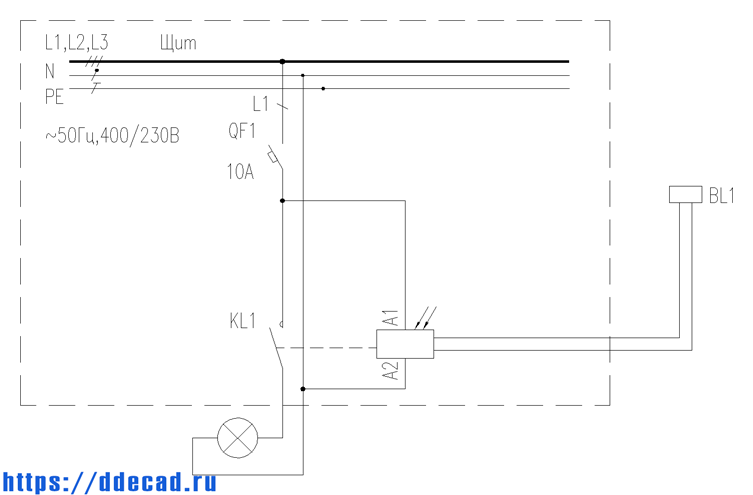
Управление наружным освещением при помощи фотореле. Базовая схема
В линейках ведущих производителей представлено несколько вариаций фотореле:
- Самая простая версия — фотореле реагирует только на уровень освещенности. Реле комплектуется фотодатчиком;
- Версия с возможностью задать программу включения (одну или несколько). Фотореле замыкает и размыкает свои контакты в зависимости от уровня освещенности и в соответствии с заданной программой. Реле комплектуется фотодатчиком;
- Астрореле. Реле фотодатчиком не комплектуется. Управление включение осуществляется по заданным программам. Время восхода и заката реле определяет автоматически в зависимости от заданных географических высоты, долготы и астрономического времени.
Как видим, по своему функционалу программируемые фотореле являются своего рода реле времени с дополнительными функциями.
На практике базовая схема управления наружным освещением обычное не применяется, т.к. необходимо одновременно включать сразу несколько групповых линий. Установка на каждую групповую линию фотореле нецелесообразно как с экономической точки зрения, так и с точки зрения здравого смысла. Поэтому в щитах наружного освещения и шкафах управления наружным освещением устанавливают одно фотореле, которое управляет питанием катушек контакторов, замыкающих силовые цепи.
Рассмотрим работу доработанной версии схемы управления наружным освещением.

Управление наружным освещением при помощи фотореле и контакторов
Питание на катушки контакторов 1KM1, 2KM1, 3KM1 подаётся через трехпозиционный переключатель SA1 с нейтральным положением:
- В положении «Ручное» питание напрямую подаётся на катушки контакторов KM и они замыкают свои пары контактов, наружное освещение включается вне зависимости от уровня освещённости
- В положении «0» цепь питания катушек контакторов разорвана и наружное освещение отключено вне зависимости от уровня освещённости
- В положении «Автомат» питание на катушки контакторов подаётся через контакты фотореле KL1. Включением и отключением наружного освещения управляет фотореле, замыкая и размыкая свои контакты в зависимости от уровня освещённости.
При необходимости, можно дополнить схему сигнальной лампой HL, включенной параллельно катушкам контакторов, которая будет информировать о включении наружного освещения.
Фотореле с несколькими программами имеет количество пар контактов в соответствии с количеством предусмотренных программ. Таким образом, можно запрограммировать несколько групп включения наружного освещения.
Управление освещением с использованием реле напряжения
Реле напряжения предназначено для других целей, но мы его будем использовать для управление освещением.
Допустим, при пропадании напряжения (снижении ниже допустимого значения и/или повышении выше допустимого значения) в щите рабочего освещения необходимо включить аварийное освещение в щите аварийного освещения.
Для этого на вводе в щит Щит1 устанавливаем реле напряжения SQZ3 производства ABB (KV1). Данное реле имеет перекидной контакт. При выходе напряжения в сети за допустимые пределы, а также при обрыве любой из фаз, реле меняет положение контактов. Выводим контакты 3 и 5 на клеммы X1:1 и X1:2 для удобства подключения сигнального кабеля.
В щите Щит2 реализована стандартная схема управления освещением при помощи контактора. Сигнальный кабель от щита Щит1 подключаем на клеммы в щит Щит2 в цепь управления питанием катушки контактора KM1.

Управление освещением при помощи реле напряжения с NO контактами
При срабатывании реле KV1 в щите Щит1 реле меняет положение контактов и пара контактов 3 и 5 становится замкнутой. Таким образом, цепь питания катушки контактора KM1 в щите Щит2 замыкается, на катушку подаётся напряжение и контактор KM1 замыкает свою пару контактов. Силовая цепь замыкается, включается освещение, подключенное к щиту Щит2.
При возвращении напряжения на вводе в щит Щит1 в допустимые пределы, реле KV1 возвращает свои контакты в исходное положение, размыкая пару контактов 3 и 5. Цепь питания катушки контактора KM1 размыкается, напряжение с катушки контактора снимается и он размыкает свои контакты. Силовая цепь размыкается, освещение, подключенное к щиту Щит2, отключается.
Вместо реле напряжения SQZ3 можно взять аналог у другого производителя, либо установить несколько реле (реле минимального напряжения, реле максимального напряжения, реле контроля фаз), а их управляющие NO-контакты соединить параллельно. Таким образом, при срабатывании любого реле будет генерироваться управляющий сигнал на включение освещения в щите Щит2.
Для большей надежности и страховки от обрыва сигнального кабеля используют схему с нормально закрытыми NC контактами.

Управление освещением при помощи реле напряжения с NC контактами
Принцип работы данной схемы аналогичен предыдущей с единственным отличием, что мы используем нормально закрытые NC контакты в цепи управления. В нормальном режиме (без напряжения на катушке) контакты контактора KM1 замкнуты. Но, т.к., мы используем NC контакт реле напряжения KV1, то в нормальном режиме катушка контактора KM1 в щите Щит2 оказывается под напряжением и размыкает свои контакты. Соответственно, цепь питания контакторов 1KM1, 2KM1 в щите Щит2 разомкнута, питание с их катушек снято и их контакты разомкнуты. Силовая цепь питания освещения, подключенного к щиту Щит2 разомкнута и освещение отключено.
При срабатывании реле напряжения KV1 в щите Щит1 пара контактов 4 и 5 размыкается и, тем самым, разрывается цепь питания катушки KM1 в щите Щит2. Без напряжения NC контакты контактора KM1 возвращаются в исходное положение — замыкаются, тем самым на катушки контакторов 1KM1, 2KM1 подается напряжение и они замыкают свои контакты. Силовая цепь питания освещения замыкается и освещение включается.
Вместо реле напряжения SQZ3 можно взять аналог у другого производителя, либо установить несколько реле (реле минимального напряжения, реле максимального напряжения, реле контроля фаз), а их управляющие NC-контакты соединить последовательно. Таким образом, при срабатывании любого реле либо обрыве сигнального кабеля будет генерироваться управляющий сигнал на включение освещения в щите Щит2, т.к. будет разрываться сеть питания катушки управляющего контактора KM1 с NC-контактами.
Управление освещением с использованием датчиков движения
Датчики движения давно перестали быть чем-то дорогим и экзотическим. Их давно уже применяют для управления освещением и экономии электроэнергии в общественных зданиях (например, в санузлах) и в загородных домах (в основном для управления наружным освещением).
Датчик представляет собой миниконтактор, который замыкает свои контакты при обнаружении движения в контролируемой зоне.
Как и с обычным выключателем, датчик следует подключать до светильника так, чтобы при его разомкнутых контактах, светильник оказывался без напряжения.
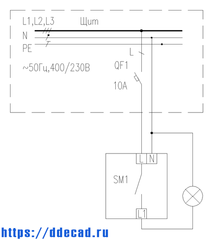
Управление освещением датчиком движения. Базовая схема
Для одновременного управления несколькими группами или для управления трехфазным группами датчики движения используют совместно с контакторами. Контакт датчик SM1 подключают в цепь питания катушки контактора KM1. При срабатывании датчика (обнаружено движение в контролируемой зоне) датчик замыкает свои контакты. Цепь питания катушки контактора KM1, на катушку подается напряжение. Контактор KM1 замыкает свои контакты, силовая цепь замыкается и включается освещение.
При размыкании контактов датчика движения SM1, цепь питания катушки контактора KM1 размыкаетя, с неё снимается напряжение. Контактор размыкает свою пару контактов и разрывает силовую цепь питания освещения. Освещение отключается.

Управление освещением датчиком движения и контактором
При управлении несколькими группами, катушки их контакторов подключаются в схему параллельно.
Также можно реализовать управление освещением по сигналу от нескольких датчиков движения. Контакты датчиков подключаются параллельно на клеммы X1:1, X1:2. При срабатывании любого из датчиков будет замкнута управляющая цепь, подано питание на катушки контакторов и, как следствие, включено освещение.
Управление освещением с использованием контроллеров
На больших объектах управление освещением осуществляют по командам из BMS — Building Management System — Системы управления зданием. Программы управления освещением записаны в контроллерах, контроллеры выдают управляющие сигналы в щиты освещения. В щитах освещения для включения и отключения освещения применены схемы с контакторами.
Скачать примеры схем управления освещением
Для получения чертежа dwg с примерами схем управления освещением из этой статьи заполните контактные данные в форме и на указанный email придёт письмо со ссылкой на скачивание файла.
Источник

World Class Design | World Class Function | 30 Years Expertise In Industrial Motor Control
HG102633v6.00a Combined
PRODUCT MANUAL:
PL/X DIGITAL DC DRIVE
PARTS 1, 2, 3 & BLOCKS
Contents
3
NOTE. These instructions do not purport to cover all details or variations in equipment, or to provide for every
possible contingency to be met in connection with installation, operation, or maintenance. Should further
information be desired or should particular problems arise which are not covered sufficiently for the purchaser's
purposes, the matter should be referred to the local Supplier sales office. The contents of this instruction manual
shall not become part of or modify any prior or existing agreement, commitment, or relationship. The sales
contract contains the entire obligation of Sprint Electric Ltd. The warranty contained in the contract between
the parties is the sole warranty of Sprint Electric Ltd. Any statements contained herein do not create new
warranties or modify the existing warranty.
IMPORTANT MESSAGE This is a version 6.00a manual. Version 6.10 and above software has all the functions
described.
See 5.1.7 Finding the software version number of the unit. DO YOU NEED HELP? See 14.13 What
to do in the event of a problem. Other PL/X manuals. Part 2 APPLICATION BLOCKS, Part 3 PL/X 275-980 (from
650A to 2250A), SERIAL COMMS and STACK DRIVER. All also available to download from www.sprint-electric.com
For the PILOT+ online configuration tool please refer to the PILOT+ Manual .
Use this manual with the main PL / PLX Digital DC Drive product manuals.
1 Table of contents
1
2
Table of contents ................................................................................... 3
Warnings ............................................................................................. 13
2.1
2.2
2.3
2.4
3
General Warnings.......................................................................................................... 13
Warnings and Instructions ............................................................................................... 14
General Risks ............................................................................................................... 15
Summary of further WARNINGS ......................................................................................... 16
Introduction and Technical Data ................................................................ 19
3.1 Introduction ................................................................................................................ 20
3.2 How do they work? ........................................................................................................ 20
3.2.1 Useful things to know about the PL/X .............................................................................. 21
3.2.2 Tips for using the manual ............................................................................................. 21
3.3 General Technical Data .................................................................................................. 22
3.3.1 Regenerative stopping with PL models ............................................................................. 22
3.3.2 Supply voltages required for all models ............................................................................ 22
3.3.3 Control terminals electrical specification......................................................................... 24
3.4 Control terminals overview.............................................................................................. 25
3.4.1 General requirements ................................................................................................. 25
3.4.2 Digital inputs and outputs............................................................................................. 25
3.4.2.1 Encoder inputs.................................................................................................... 26
3.4.2.2 Digital outputs.................................................................................................... 26
3.4.3 Analogue inputs ......................................................................................................... 26
3.4.4 Analogue tachogenerator input ...................................................................................... 27
3.4.5 Signal test pins .......................................................................................................... 27
3.5 Control terminal default functions..................................................................................... 27
3.5.1 Run, Jog, Start, Cstop ................................................................................................. 29
3.5.2 Summary of default terminal functions ............................................................................ 31
3.6 Supply loss shutdown ..................................................................................................... 32
3.7 PILOT+ ....................................................................................................................... 32
4
Basic application ................................................................................... 33
4.1 Basic speed or torque control ........................................................................................... 34
4.2 Main Contactor operation................................................................................................ 35
4.2.1 Contactor control questions and answers .......................................................................... 35
4.3 Main contactor wiring options .......................................................................................... 37
4.3.1 Main contactor isolating AC stack supply........................................................................... 37
4.3.2 Main contactor isolating AC stack and auxiliary supplies........................................................ 37
4
Contents
4.3.3 Main contactor isolating DC armature .............................................................................. 38
4.3.4 Using pushbuttons for simple STOP / START (Coast to stop) ................................................... 39
4.3.5 Using pushbuttons for STOP / START (With ramp to stop, jog and slack take up) .......................... 40
4.4 ESSENTIAL pre-start checks.............................................................................................. 41
4.4.1 POWER ENGINEERING .................................................................................................. 41
4.4.2 MECHANICAL ENGINEERING ........................................................................................... 41
4.5 CONTROL ENGINEERING COMMISSIONING PROCEDURES............................................................. 42
4.5.1 Quick start calibration ................................................................................................. 42
4.5.2 Quick start calibration step by step ................................................................................. 43
4.5.3 Quick start current loop AUTOTUNE ................................................................................. 43
4.5.4 PASSIVE MOTOR defaults / Using passive motor menu for small test motors ................................ 44
5
Menu tree structure ............................................................................... 45
5.1 Key functions ............................................................................................................... 46
5.1.1 Incrementing and decrementing parameter values. ............................................................. 47
5.1.2 PARAMETER SAVE ....................................................................................................... 47
5.1.3 Restoring the drive parameters to the default condition ....................................................... 47
5.1.4 Branch hopping between monitor windows ........................................................................ 47
5.1.5 Power up windows...................................................................................................... 47
5.1.6 Default % DIAGNOSTIC summary windows .......................................................................... 48
5.1.7 Finding the software version number of the unit. ................................................................ 48
5.2 ENTRY MENU................................................................................................................ 48
5.2.1 Full menu diagram (Change parameters)........................................................................... 49
5.2.2 Full menu diagram (Change parameters continued) ............................................................. 50
5.2.3 Full menu diagram (Diagnostics) ..................................................................................... 51
5.2.4 Full menu diagram (Motor drive alarms, serial links and display functions) ................................. 52
5.2.5 Full menu diagram (Application blocks and configuration) ..................................................... 53
5.2.6 Full menu diagram (Configuration continued)..................................................................... 54
5.2.7 Full menu diagram (Block OP and Fieldbus configs, Drive personality and Conflict Help) ................ 55
5.3 Archiving PL/X recipes ................................................................................................... 56
6
CHANGE PARAMETERS............................................................................. 57
6.1 CHANGE PARAMETERS / CALIBRATION ................................................................................. 59
6.1.1 CALIBRATION / Block diagram........................................................................................ 60
6.1.2 CALIBRATION / Rated armature amps PIN 2 QUICK START................................................... 60
6.1.3 CALIBRATION / Current limit (%) PIN 3 QUICK START ......................................................... 61
6.1.4 CALIBRATION / Rated field amps PIN 4 QUICK START ........................................................ 61
6.1.5 CALIBRATION / Base rated motor rpm PIN 5 QUICK START .................................................. 62
6.1.6 CALIBRATION / Desired max rpm PIN 6 QUICK START......................................................... 62
6.1.7 CALIBRATION / Zero speed offset PIN 7........................................................................... 62
6.1.8 CALIBRATION / Max tacho volts PIN 8 ............................................................................. 63
6.1.9 CALIBRATION / Speed feedback type PIN 9 QUICK START ................................................... 64
6.1.10 CALIBRATION / ENCODER SCALING ................................................................................. 65
6.1.10.1 ENCODER SCALING / Quadrature enable PIN 10 ......................................................... 66
6.1.10.2 ENCODER SCALING / Encoder lines PIN 11................................................................ 67
6.1.10.3 ENCODER SCALING / Motor / encoder speed ratio PIN 12 ............................................. 67
6.1.10.4 ENCODER SCALING / Encoder sign PIN 13................................................................. 67
6.1.11 CALIBRATION / IR compensation PIN 14 ......................................................................... 68
6.1.12 CALIBRATION / Field current feedback trim PIN 15 ........................................................... 68
6.1.13 CALIBRATION / Armature volts trim PIN 16 ..................................................................... 68
6.1.14 CALIBRATION / Analog tacho trim PIN 17 ....................................................................... 69
6.1.15 CALIBRATION / Rated armature volts PIN 18 QUICK START ................................................ 69
6.1.16 CALIBRATION / EL1/2/3 rated AC volts PIN 19 QUICK START .............................................. 69
6.1.17 CALIBRATION / Motor 1 or 2 select PIN 20 ...................................................................... 70
6.2 CHANGE PARAMETERS / RUN MODE RAMPS ........................................................................... 71
6.2.1 RUN MODE RAMPS / Block diagram including JOG ................................................................ 72
6.2.2 RUN MODE RAMPS / Ramp output monitor PIN 21............................................................... 73
6.2.3 RUN MODE RAMPS / Forward up time PIN 22..................................................................... 73
6.2.4 RUN MODE RAMPS / Forward down time PIN 23 ................................................................. 73
6.2.5 RUN MODE RAMPS / Reverse up time PIN 24 ..................................................................... 73
6.2.6 RUN MODE RAMPS / Reverse down time PIN 25.................................................................. 73
6.2.7 RUN MODE RAMPS / Ramp input PIN 26 ........................................................................... 74
Contents
5
6.2.8 RUN MODE RAMPS / Forward minimum speed PIN 27........................................................... 74
6.2.9 RUN MODE RAMPS / Reverse minimum speed PIN 28 ........................................................... 74
6.2.10 RUN MODE RAMPS / Ramp automatic preset PIN 29 ........................................................... 75
6.2.11 RUN MODE RAMPS / Ramp external preset PIN 30 ............................................................. 75
6.2.12 RUN MODE RAMPS / Ramp preset value PIN 31 ................................................................. 75
6.2.13 RUN MODE RAMPS / Ramp S-profile % PIN 32 ................................................................... 75
6.2.14 RUN MODE RAMPS / Ramp hold enable PIN 33.................................................................. 75
6.2.15 RUN MODE RAMPS / Ramping threshold PIN 34................................................................. 76
6.2.16 RUN MODE RAMPS / Ramping flag PIN 35........................................................................ 76
6.3 CHANGE PARAMETERS / JOG CRAWL SLACK .......................................................................... 77
6.3.1 JOG CRAWL SLACK / Block diagram including RUN MODE RAMPS .............................................. 78
6.3.2 JOG CRAWL SLACK / Jog speed 1 / 2 PINs 37 / 38.............................................................. 79
6.3.3 JOG CRAWL SLACK / Slack speed 1 / 2 PINs 39 / 40............................................................ 79
6.3.4 JOG CRAWL SLACK / Crawl speed PIN 41 ......................................................................... 79
6.3.5 JOG CRAWL SLACK / Jog mode select PIN 42 .................................................................... 80
6.3.6 JOG CRAWL SLACK / Jog/Slack ramp PIN 43 ..................................................................... 80
6.4 CHANGE PARAMETERS / MOTORISED POT RAMP...................................................................... 81
6.4.1 MOTORISED POT RAMP / Block diagram ............................................................................ 82
6.4.2 MOTORISED POT RAMP / MP output monitor PIN 45 ............................................................ 82
6.4.3 MOTORISED POT RAMP / MP Up / Down time PINs 46 / 47 .................................................... 82
6.4.4 MOTORISED POT RAMP / MP Up / Down command PINs 48 / 49 .............................................. 83
6.4.5 MOTORISED POT RAMP / MP Maximum / minimum clamps PINs 50 / 51 .................................... 83
6.4.6 MOTORISED POT RAMP / MP preset PIN 52 ....................................................................... 83
6.4.7 MOTORISED POT RAMP / MP Preset value PIN 53................................................................ 84
6.4.8 MOTORISED POT RAMP / MP memory boot up PIN 54........................................................... 84
6.5 CHANGE PARAMETERS / STOP MODE RAMP ........................................................................... 85
6.5.1 STOP MODE RAMP / Block diagram .................................................................................. 85
6.5.1.1 Block diagram of contactor control........................................................................... 86
6.5.1.2 Speed profile when stopping................................................................................... 87
6.5.1.3 Contactor drop out .............................................................................................. 87
6.5.1.4 Precise stopping.................................................................................................. 88
6.5.2 STOP MODE RAMP / Stop ramp time PIN 56 ...................................................................... 88
6.5.3 STOP MODE RAMP / Stop time limit PIN 57....................................................................... 88
6.5.4 STOP MODE RAMP / Live delay mode PIN 58 ..................................................................... 89
6.5.5 STOP MODE RAMP / Drop-out speed PIN 59 ...................................................................... 89
6.5.6 STOP MODE RAMP / Drop-out delay PIN 60 ....................................................................... 89
6.6 CHANGE PARAMETERS / SPEED REF SUMMER ......................................................................... 90
6.6.1 SPEED REF SUMMER / Block diagram ................................................................................ 90
6.6.2 SPEED REF SUMMER / Internal speed reference 1 PIN 62 ...................................................... 91
6.6.3 SPEED REF SUMMER / Auxiliary speed reference 2 PIN 63 ..................................................... 91
6.6.4 SPEED REF SUMMER / Speed reference 3 monitor PIN 64 ...................................................... 91
6.6.5 SPEED REF SUMMER / Ramped speed reference 4 PIN 65 ...................................................... 91
6.6.6 SPEED REF SUMMER / Speed/Current Reference 3 sign PIN 66 ............................................... 91
6.6.7 SPEED REF SUMMER / Speed/Current Reference 3 ratio PIN 67 .............................................. 92
6.7 CHANGE PARAMETERS / SPEED CONTROL ............................................................................. 92
6.7.1 SPEED CONTROL / Block diagram .................................................................................... 93
6.7.2 SPEED CONTROL / Max positive speed reference PIN 69....................................................... 93
6.7.3 SPEED CONTROL / Max negative speed reference PIN 70...................................................... 93
6.7.4 SPEED CONTROL / Speed proportional gain PIN 71 ............................................................. 93
6.7.5 SPEED CONTROL / Speed integral time constant PIN 72 ....................................................... 94
6.7.6 SPEED CONTROL / Speed integral reset enable PIN 73......................................................... 94
6.7.7 SPEED CONTROL / SPEED PI ADAPTION ............................................................................. 94
6.7.7.1 SPEED PI ADAPTION / Low break point PIN 74 ............................................................ 95
6.7.7.2 SPEED PI ADAPTION / High break point PIN 75............................................................ 95
6.7.7.3 SPEED PI ADAPTION / Low breakpoint proportional gain PIN 76 ....................................... 95
6.7.7.4 SPEED PI ADAPTION / Low breakpoint integral time constant PIN 77................................. 95
6.7.7.5 SPEED PI ADAPTION / Integral % during ramp PIN 78 .................................................... 95
6.7.7.6 SPEED PI ADAPTION / Speed loop adaption enable PIN 79.............................................. 96
6.7.7.7 SPEED PI ADAPTION / Using small speed inputs ............................................................ 96
6.8 CHANGE PARAMETERS / CURRENT CONTROL ......................................................................... 97
6.8.1 CURRENT CONTROL / Block diagram ................................................................................ 98
6
Contents
6.8.2 CURRENT CONTROL / Current clamp scaler PIN 81 ............................................................. 98
6.8.3 CURRENT CONTROL / CURRENT OVERLOAD ........................................................................ 98
6.8.3.1 CURRENT OVERLOAD / Overload % target PIN 82 ......................................................... 99
6.8.3.1.1 Diagram showing O/LOAD % TARGET set to 105% ..................................................... 99
6.8.3.1.2 How to get overloads greater than 150% using 82)O/LOAD % TARGET .......................... 100
6.8.3.1.3 Maximum overload table ................................................................................ 100
6.8.3.2 CURRENT OVERLOAD / Overload ramp time PIN 83 .................................................... 100
6.8.4 CURRENT CONTROL / I DYNAMIC PROFILE........................................................................ 101
6.8.4.1 I DYNAMIC PROFILE / Profile enable PIN 84 ............................................................. 101
6.8.4.2 I DYNAMIC PROFILE / Speed break point for high current limit PIN 85 .............................. 102
6.8.4.3 I DYNAMIC PROFILE / Speed break point for low current limit PIN 86 ............................... 102
6.8.4.4 I DYNAMIC PROFILE / Profile current for low current limit PIN 87 .................................. 102
6.8.5 CURRENT CONTROL / Dual current clamps enable PIN 88 ................................................... 102
6.8.6 CURRENT CONTROL / Upper current clamp PIN 89 ........................................................... 103
6.8.7 CURRENT CONTROL / Lower current clamp PIN 90 ........................................................... 103
6.8.8 CURRENT CONTROL / Extra current reference PIN 91........................................................ 103
6.8.9 CURRENT CONTROL / Autotune enable PIN 92 ................................................................ 103
6.8.10 CURRENT CONTROL / Current amp proportional gain PIN 93 .............................................. 104
6.8.11 CURRENT CONTROL / Current amp integral gain PIN 94.................................................... 104
6.8.12 CURRENT CONTROL / Discontinuous current point PIN 95 ................................................. 105
6.8.12.1 Setting the current loop control terms manually. ...................................................... 105
6.8.13 CURRENT CONTROL / 4 quadrant mode enable PIN 96 ..................................................... 105
6.8.14 CURRENT CONTROL / Speed bypass current reference enable PIN 97 ................................... 105
6.9 CHANGE PARAMETERS / FIELD CONTROL ............................................................................ 106
6.9.1 FIELD CONTROL / Block diagram................................................................................... 107
6.9.2 FIELD CONTROL / Field enable PIN 99 .......................................................................... 108
6.9.3 FIELD CONTROL / Voltage output % PIN 100 ................................................................... 108
6.9.4 FIELD CONTROL / Field proportional gain PIN 101 ............................................................ 108
6.9.5 FIELD CONTROL / Field integral gain PIN 102.................................................................. 108
6.9.6 FIELD CONTROL / FLD WEAKENING MENU ........................................................................ 109
6.9.6.1 FLD WEAKENING MENU / Field weakening enable PIN 103............................................ 110
6.9.6.2 FLD WEAKENING MENU / Field weakening proportional gain PIN 104............................... 110
6.9.6.3 FLD WEAKENING MENU / Field weakening integral time constant PIN 105 ........................ 110
6.9.6.4 FLD WEAKENING MENU / Field weakening derivative time constant PIN 106 ..................... 110
6.9.6.5 FLD WEAKENING MENU / Field weakening feedback derivative time constant PIN 107 ......... 111
6.9.6.6 FLD WEAKENING MENU / Field weakening feedback integral time constant PIN 108 ............ 111
6.9.6.7 FLD WEAKENING MENU / Spillover armature voltage % PIN 109 ..................................... 111
6.9.6.8 FLD WEAKENING MENU / Minimum field current % PIN 110 ........................................... 111
6.9.7 FIELD CONTROL / Standby field enable PIN 111............................................................... 112
6.9.8 FIELD CONTROL / Standby field current PIN 112 .............................................................. 112
6.9.9 FIELD CONTROL / Quench delay PIN 113 ....................................................................... 112
6.9.10 FIELD CONTROL / Field reference input PIN 114............................................................. 112
6.10 CHANGE PARAMETERS / ZERO INTERLOCKS ........................................................................ 113
6.10.1 ZERO INTERLOCKS / Block diagram .............................................................................. 114
6.10.2 ZERO INTERLOCKS / Standstill enable PIN 115 ............................................................... 114
6.10.3 ZERO INTERLOCKS / Zero reference start enable PIN 116.................................................. 114
6.10.4 ZERO INTERLOCKS / Zero interlocks speed level PIN 117 .................................................. 114
6.10.5 ZERO INTERLOCKS / Zero interlocks current level PIN 118................................................. 115
6.10.6 ZERO INTERLOCKS / At zero reference flag PIN 119......................................................... 115
6.10.7 ZERO INTERLOCKS / At zero speed flag PIN 120 ............................................................. 115
6.10.8 ZERO INTERLOCKS / At standstill flag PIN 121................................................................ 115
6.10.8.1 Low speed performance ..................................................................................... 115
6.10.9 ZERO INTERLOCKS / SPINDLE ORIENTATE ....................................................................... 116
6.10.9.1 SPINDLE ORIENTATE / Block diagram ..................................................................... 117
6.10.9.1.1 Spindle orientate operation ........................................................................... 117
6.10.9.2 SPINDLE ORIENTATE / Zero speed lock PIN 122 ....................................................... 118
6.10.9.3 SPINDLE ORIENTATE / Marker enable PIN 240 ......................................................... 118
6.10.9.3.1 Marker specification .................................................................................... 118
6.10.9.4 SPINDLE ORIENTATE / Marker offset PIN 241 .......................................................... 119
6.10.9.5 SPINDLE ORIENTATE / Position reference PIN 242 .................................................... 120
6.10.9.6 SPINDLE ORIENTATE / Marker frequency monitor PIN 243 .......................................... 120
Contents
6.10.9.7
7
7
SPINDLE ORIENTATE / In position flag PIN 244 ........................................................ 120
DIAGNOSTICS ...................................................................................... 121
7.1 DIAGNOSTICS / SPEED LOOP MONITOR...............................................................................
7.1.1 SPEED LOOP MONITOR / Total speed reference monitor PIN 123 ..........................................
7.1.2 SPEED LOOP MONITOR / Speed demand monitor PIN 124....................................................
7.1.3 SPEED LOOP MONITOR / Speed error monitor PIN 125 .......................................................
7.1.4 SPEED LOOP MONITOR / Armature volts monitor PIN 126 ...................................................
7.1.5 SPEED LOOP MONITOR / Armature volts % monitor PIN 127.................................................
7.1.6 SPEED LOOP MONITOR / Back emf % monitor PIN 128........................................................
7.1.7 SPEED LOOP MONITOR / Tachogenerator volts monitor PIN 129 ...........................................
7.1.8 SPEED LOOP MONITOR / Motor RPM monitor PIN 130.........................................................
7.1.9 SPEED LOOP MONITOR / Encoder RPM monitor PIN 132......................................................
7.1.10 SPEED LOOP MONITOR / Speed feedback % monitor PIN 131 ..............................................
7.2 DIAGNOSTICS / ARM I LOOP MONITOR ...............................................................................
7.2.1 ARM I LOOP MONITOR / Armature current demand monitor PIN 133 ......................................
7.2.2 ARM I LOOP MONITOR / Armature current % monitor PIN 134 ..............................................
7.2.3 ARM I LOOP MONITOR / Armature current amps monitor PIN 135 .........................................
7.2.4 ARM I LOOP MONITOR / Upper current limit monitor PIN 136 ..............................................
7.2.5 ARM I LOOP MONITOR / Lower current limit monitor PIN 137 ..............................................
7.2.6 ARM I LOOP MONITOR / Actual prevailing upper/ lower current limits PINs 138 / 139 ................
7.2.7 ARM I LOOP MONITOR / Overload limit monitor PIN 140.....................................................
7.2.8 ARM I LOOP MONITOR / At current limit flag PIN 141 ........................................................
7.3 DIAGNOSTICS / FLD I LOOP MONITOR ................................................................................
7.3.1 FLD I LOOP MONITOR / Field demand monitor PIN 143 ......................................................
7.3.2 FLD I LOOP MONITOR / Field current % monitor PIN 144 ....................................................
7.3.3 FLD I LOOP MONITOR / Field current amps monitor PIN 145................................................
7.3.4 FLD I LOOP MONITOR / Field firing angle of advance monitor PIN 146....................................
7.3.5 FLD I LOOP MONITOR / Field active monitor PIN 147 ........................................................
7.4 DIAGNOSTICS / ANALOG IO MONITOR ................................................................................
7.4.1 ANALOG IO MONITOR / UIP2 to 9 analogue input monitor PINs 150 to 157................................
7.4.2 ANALOG IO MONITOR / AOP1/2/3 analogue output monitor PINs 159, 160, 161 ........................
7.5 DIAGNOSTICS / DIGITAL IO MONITOR ................................................................................
7.5.1 DIGITAL IO MONITOR / UIP2 to 9 digital input monitor PIN 162 ............................................
7.5.2 DIGITAL IO MONITOR / DIP1 to 4 and DIO1 to 4 digital input monitor PIN 163...........................
7.5.3 DIGITAL IO MONITOR / DOP1 to 3 + Control IPs digital monitor PIN 164 ..................................
7.5.4 DIGITAL IO MONITOR / +Armature bridge flag PIN 165.......................................................
7.5.5 DIGITAL IO MONITOR / Drive start flag PIN 166 ...............................................................
7.5.6 DIGITAL IO MONITOR / Drive run flag PIN 167 .................................................................
7.5.7 DIGITAL IO MONITOR / Internal running mode monitor PIN 168 ............................................
7.6 DIAGNOSTICS / BLOCK OP MONITOR .................................................................................
7.6.1 BLOCK OP MONITOR / General description ......................................................................
7.7 DIAGNOSTICS / EL1/2/3 RMS MON PIN 169 .......................................................................
7.8 DIAGNOSTICS / DC KILOWATTS MON PIN 170 ....................................................................
8
122
122
123
123
123
123
123
124
124
124
124
125
126
126
126
126
126
127
127
127
128
128
128
128
129
129
130
130
130
131
131
131
132
132
132
132
132
133
134
134
134
MOTOR DRIVE ALARMS........................................................................... 135
8.1 MOTOR DRIVE ALARMS menu ..........................................................................................
8.1.1 MOTOR DRIVE ALARMS / Speed feedback mismatch trip enable PIN 171 .................................
8.1.2 MOTOR DRIVE ALARMS / Speed feedback mismatch tolerance PIN 172 ...................................
8.1.3 MOTOR DRIVE ALARMS / Field loss trip enable PIN 173 ......................................................
8.1.4 MOTOR DRIVE ALARMS / Digital OP short circuit trip enable PIN 174 .....................................
8.1.5 MOTOR DRIVE ALARMS / Missing pulse trip enable PIN 175..................................................
8.1.6 MOTOR DRIVE ALARMS / Reference exchange trip enable PIN 176.........................................
8.1.7 MOTOR DRIVE ALARMS / Overspeed delay time PIN 177 .....................................................
8.1.8 MOTOR DRIVE ALARMS / STALL TRIP MENU ......................................................................
8.1.8.1 STALL TRIP MENU / Stall trip enable PIN 178 ...........................................................
8.1.8.2 STALL TRIP MENU / Stall current level PIN 179 .........................................................
8.1.8.3 STALL TRIP MENU / Stall time PIN 180 ...................................................................
8.1.9 MOTOR DRIVE ALARMS / Active and stored trip monitors PINS 181 / 182 ................................
8.1.10 MOTOR DRIVE ALARMS / External trip reset enable PIN 183 ...............................................
8.1.11 MOTOR DRIVE ALARMS / DRIVE TRIP MESSAGE .................................................................
8.1.11.1 DRIVE TRIP MESSAGE / Armature overcurrent...........................................................
136
137
139
139
139
140
140
140
141
141
141
141
142
143
143
143
8
Contents
8.1.11.2
8.1.11.3
8.1.11.4
8.1.11.5
8.1.11.6
8.1.11.7
8.1.11.8
8.1.11.9
8.1.11.10
8.1.11.11
8.1.11.12
8.1.11.13
8.1.11.14
8.1.11.15
8.1.11.16
8.1.11.17
8.1.11.18
8.1.11.19
9
DRIVE TRIP MESSAGE / Armature overvolts .............................................................. 143
DRIVE TRIP MESSAGE / Field overcurrent ................................................................ 143
DRIVE TRIP MESSAGE / Field loss .......................................................................... 144
DRIVE TRIP MESSAGE / User trip ........................................................................... 144
DRIVE TRIP MESSAGE / Thermistor on T30 ............................................................... 144
DRIVE TRIP MESSAGE / Overspeed ......................................................................... 144
DRIVE TRIP MESSAGE / Speed feedback mismatch ..................................................... 145
DRIVE TRIP MESSAGE / Stall trip ........................................................................... 145
DRIVE TRIP MESSAGE / Missing pulse .................................................................... 145
DRIVE TRIP MESSAGE / Supply phase loss ............................................................... 145
DRIVE TRIP MESSAGE / Synchronization loss ........................................................... 146
DRIVE TRIP MESSAGE / Heatsink overtemp ............................................................. 146
DRIVE TRIP MESSAGE / Short circuit digital outputs ................................................. 146
DRIVE TRIP MESSAGE / Bad reference exchange ...................................................... 146
DRIVE TRIP MESSAGE / Cannot autotune................................................................ 147
DRIVE TRIP MESSAGE / Autotune quit ................................................................... 147
DRIVE TRIP MESSAGE / Contactor lock out ............................................................. 147
DRIVE TRIP MESSAGE / Warning flags.................................................................... 147
SELF TEST MESSAGE ..............................................................................148
9.1.1 SELF TEST MESSAGE / Data corruption............................................................................ 148
9.1.2 SELF TEST MESSAGE / Disable GOTO, GETFROM ................................................................ 148
9.1.3 SELF TEST MESSAGE / Self cal tolerance ......................................................................... 148
9.1.4 SELF TEST MESSAGE / Proportional armature current cal fail ................................................ 148
9.1.5 SELF TEST MESSAGE / Integral armature current cal fail...................................................... 148
9.1.6 SELF TEST MESSAGE / Stop drive to adjust parameter......................................................... 149
9.1.7 SELF TEST MESSAGE / Enter password ............................................................................ 149
9.1.8 SELF TEST MESSAGE / Enable GOTO, GETFROM ................................................................. 149
9.1.9 SELF TEST MESSAGE / GOTO CONFLICT ........................................................................... 149
9.1.10 SELF TEST MESSAGE / Internal error code ...................................................................... 149
9.1.11 SELF TEST MESSAGE / Authorisation needed ................................................................... 149
9.1.12 SELF TEST MESSAGE / Memory write error...................................................................... 150
9.1.13 SELF TEST MESSAGE / Memory version error ................................................................... 150
9.1.13.1 Transferring files using PILOT+............................................................................. 150
10
SERIAL LINKS, RS232 and FIELDBUS ...........................................................151
10.1 SERIAL LINKS / RS232 PORT1 ......................................................................................... 152
10.1.1 RS232 PORT1 / Connection pinouts .............................................................................. 153
10.1.2 RS232 PORT1 / Port1 Baud rate PIN 187....................................................................... 153
10.1.3 RS232 PORT1 / Port1 function PIN 188 ........................................................................ 153
10.1.4 How to use USB ports on external PC ............................................................................ 153
10.2 RS232 PORT1 / PARAMETER EXCHANGE............................................................................. 154
10.2.1 PARAMETER EXCHANGE / Drive transmit ........................................................................ 154
10.2.1.1 PARAMETER EXCHANGE with a locked recipe page 3................................................... 155
10.2.1.2 Transmitting parameter data file to a PC. Windows 95 to Windows XP. ........................... 155
10.2.2 PARAMETER EXCHANGE / Drive receive ......................................................................... 156
10.2.2.1 Receiving parameter data file from a PC. Windows 95 to Windows XP............................. 156
10.2.3 PARAMETER EXCHANGE / menu list to host..................................................................... 157
10.2.3.1 Transmitting a menu list to a PC. Windows 95 to windows XP ....................................... 157
10.2.3.2 PARAMETER EXCHANGE / Drive to drive.................................................................. 158
10.2.3.3 PARAMETER EXCHANGE / Eeprom transfer between units ............................................ 159
10.2.4 Rules of parameter exchange relating to software version.................................................. 159
10.2.4.1 PL PILOT Legacy configuration tool and SCADA ......................................................... 160
10.3 RS232 PORT1 / PORT1 REF EXCHANGE .............................................................................. 161
10.3.1 REFERENCE EXCHANGE / Reference exchange slave ratio PIN 189 ....................................... 162
10.3.2 REFERENCE EXCHANGE/ Reference exchange slave sign PIN 190 ......................................... 162
10.3.3 REFERENCE EXCHANGE / Reference exchange slave monitor PIN 191 ................................... 162
10.3.4 REFERENCE EXCHANGE / Reference exchange master monitor PIN 192 ................................. 162
10.3.5 REFERENCE EXCHANGE / Reference exchange master GET FROM .......................................... 162
11
DISPLAY FUNCTIONS ..............................................................................163
11.1
11.2
DISPLAY FUNCTIONS / Reduced menu enable ..................................................................... 163
DISPLAY FUNCTIONS / PASSWORD CONTROL....................................................................... 163
Contents
9
11.2.1 PASSWORD CONTROL / Enter password .........................................................................
11.2.2 PASSWORD CONTROL / Alter password ..........................................................................
11.3 DISPLAY FUNCTIONS / Language select.............................................................................
11.4 DISPLAY FUNCTIONS / Software version ............................................................................
11.5 Remotely mounted display unit ......................................................................................
12
APPLICATION BLOCKS ........................................................................... 165
12.1 General rules ............................................................................................................
12.1.1 Sample times .........................................................................................................
12.1.2 Order of processing .................................................................................................
12.1.3 Logic levels ...........................................................................................................
12.1.4 Activating blocks ....................................................................................................
12.1.4.1 Conflicting GOTO connections .............................................................................
12.1.4.2 Application blocks PIN table................................................................................
13
164
164
164
164
164
165
165
165
166
166
166
166
CONFIGURATION .................................................................................. 167
13.1 Driveweb Ethernet Connectivity and PILOT+ configuration tool ...............................................
13.2 CONFIGURATION menu.................................................................................................
13.2.1 PL PILOT legacy configuration tool..............................................................................
13.3 Configurable connections .............................................................................................
13.3.1 Key features of GOTO window ....................................................................................
13.3.2 Key features of GET FROM window...............................................................................
13.3.3 Summary of GOTO and GET FROM windows ....................................................................
13.3.4 JUMPER connections ................................................................................................
13.3.5 Block Disconnect PIN 400.........................................................................................
13.3.6 Hidden parameters..................................................................................................
13.3.7 CONFIGURATION / ENABLE GOTO, GETFROM...................................................................
13.4 CONFIGURATION / UNIVERSAL INPUTS ..............................................................................
13.4.1 UNIVERSAL INPUTS / Block diagram..............................................................................
13.4.1.1 UIPX SETUP / UIP(2) to (9) Input range PIN 3(2)0 to 3(9)0 ..........................................
13.4.1.2 UIPX SETUP / UIP(2) to (9) Input offset PIN 3(2)1 to 3(9)1 ..........................................
13.4.1.2.1 4-20mA loop input SETUP ..............................................................................
13.4.1.3 UIPX SETUP / UIP(2) to (9) Linear scaling ratio PIN 3(2)2 to 3(9)2.................................
13.4.1.4 UIPX SETUP / UIP(2) to (9) Maximum clamp level PIN 3(2)3 to 3(9)3 .............................
13.4.1.5 UIPX SETUP / UIP(2) to (9) Minimum clamp level PIN 3(2)4 to 3(9)4 ..............................
13.4.1.6 UIPX SETUP / UIP(2) to (9) Make analog GOTO destination connection ............................
13.4.1.7 UIPX SETUP / UIP(2) to (9) Make digital output 1 GOTO destination connection .................
13.4.1.8 UIPX SETUP / UIP(2) to (9) Make digital output 2 GOTO destination connection .................
13.4.1.9 UIPX SETUP / UIP(2) to (9) Digital input, high value for output 1 PIN 3(2)5 to 3(9)5...........
13.4.1.10 UIPX SETUP / UIP(2) to (9) Digital input, low value for output 1 PIN 3(2)6 to 3(9)6 ..........
13.4.1.11 UIPX SETUP / UIP(2) to (9) Digital input, high value for output 2 PIN 3(2)7 to 3(9)7 .........
13.4.1.12 UIPX SETUP / UIP(2) to (9) Digital input, low value for output 2 PIN 3(2)8 to 3(9)8 ..........
13.4.1.13 UIPX SETUP / UIP(2) to (9) Threshold PIN 3(2)9 to 3(9)9...........................................
13.5 CONFIGURATION / ANALOG OUTPUTS ..............................................................................
13.5.1 ANALOG OUTPUTS / AOP4 Iarm output rectify enable PIN 250 ...........................................
13.5.2 ANALOG OUTPUTS / AOP1/2/3/4 SETUP........................................................................
13.5.2.1 AOPX SETUP / AOP1/2/3 Dividing factor
PINs 251 / 254 / 257 ...................................
13.5.2.2 AOPX SETUP / AOP1/2/3 Offset
PINs 252 / 255 / 258..............................................
13.5.2.3 AOPX SETUP / AOP1/2/3 Rectify mode enable
PINs 253 / 256 / 259............................
13.5.2.4 AOPX SETUP / AOP1/2/3 Make output GET FROM source connection ..............................
13.5.2.5 Default connections for AOP1/2/3 ........................................................................
13.5.3 ANALOG OUTPUTS / Scope output select PIN 260 ...........................................................
13.6 CONFIGURATION / DIGITAL INPUTS..................................................................................
13.6.1 Using DIP inputs for encoder signals. ............................................................................
13.6.2 DIGITAL INPUTS / DIPX SETUP.....................................................................................
13.6.2.1 DIPX SETUP / DIP1/2/3/4 Input high value PINs 310 / 312 / 314 / 316 ..........................
13.6.2.2 DIPX SETUP / DIP1/2/3/4 Input low value PINs 311 / 313 / 315 / 317...........................
13.6.2.3 DIPX SETUP / DIP1/2/3/4 Make input value GOTO destination connection........................
13.6.2.4 Default connections for DIP1/2/3/4 ......................................................................
13.6.3 DIGITAL INPUTS / RUN INPUT SETUP.............................................................................
13.6.3.1 RUN INPUT SETUP / RUN input HI value PIN 318 ......................................................
13.6.3.2 RUN INPUT SETUP / RUN input LO value PIN 319 .....................................................
167
168
168
169
170
170
171
171
171
171
172
172
174
174
174
175
175
175
175
176
176
176
177
177
177
177
177
178
178
178
179
179
179
179
179
180
180
180
181
181
181
181
181
182
182
182
10
Contents
13.6.3.3 RUN INPUT SETUP / Make input value GOTO destination connection............................... 182
13.7 CONFIGURATION / DIGITAL IN/OUTPUTS ........................................................................... 183
13.7.1 DIGITAL IN/OUTPUTS / DIOX SETUP.............................................................................. 183
13.7.1.1 DIOX SETUP / DIO1/2/3/4 Output mode enable PINs 271 / 277 / 283 / 289..................... 184
13.7.1.2 DIOX SETUP / DIO1/2/3/4 OP val rectify enable PINs 272/ 278 / 284 /290...................... 184
13.7.1.3 DIOX SETUP / DIO1/2/3/4 OP comp threshold PINs 273 / 279 / 285 / 290....................... 184
13.7.1.4 DIOX SETUP / DIO1/2/3/4 OP inversion PINs 274 / 280 / 286 / 291............................... 184
13.7.1.5 DIOX SETUP / DIO1/2/3/4 Make output GET FROM source connection ............................. 185
13.7.1.6 DIOX SETUP / DIO1/2/3/4 Make input GOTO destination connection............................... 185
13.7.1.7 DIOX SETUP / DIO1/2/3/4 Input high value PINs 275 / 281 / 287 / 293 ......................... 185
13.7.1.8 DIOX SETUP / DIO1/2/3/4 Input low value PINs 276 / 282 / 288 / 294 .......................... 186
13.7.1.9 Default connections for DIO1/2/3/4 ...................................................................... 186
13.7.1.10 DIO1/2/3/4 Internal output result PINs 685/6/7/8 ................................................... 186
13.8 CONFIGURATION / DIGITAL OUTPUTS ............................................................................... 186
13.8.1
DIGITAL OUTPUTS / DOPX SETUP ................................................................................ 186
13.8.1.1 DOPX SETUP / DOP1/2/3 OP val rectifiy enable PINs 261 / 264 / 267 ............................ 187
13.8.1.2 DOPX SETUP / DOP1/2/3 OP comparator threshold PINs 262 / 265 / 268 ........................ 187
13.8.1.3 DOPX SETUP / DOP1/2/3 Output inversion enable PINs 263 / 266 / 269 ......................... 187
13.8.1.4 DOPX SETUP / DOP1/2/3 Make output GET FROM source connection .............................. 187
13.8.1.5 Default connections for DOP1/2/3 ........................................................................ 188
13.8.1.6 DOP1/2/3 Internal output result PINs 682/3/4 ......................................................... 188
13.9 CONFIGURATION / STAGING POSTS.................................................................................. 188
13.9.1 Connecting PINs with different units ............................................................................ 189
13.9.1.1 Connecting linear values with different units ........................................................... 189
13.9.1.2 Connecting logic values with different messages....................................................... 189
13.9.1.3 Connecting to multi-state logic parameters ............................................................. 190
13.9.2 STAGING POSTS / Digital / analog 1/2/3/4 PINs 296 to 303 ............................................... 190
13.10 CONFIGURATION / SOFTWARE TERMINALS ......................................................................... 191
13.10.1 SOFTWARE TERMINALS / Anded run PIN 305................................................................. 191
13.10.2 SOFTWARE TERMINALS / Anded jog PIN 306 ................................................................. 191
13.10.3 SOFTWARE TERMINALS / Anded start PIN 307 ............................................................... 192
13.10.4 SOFTWARE TERMINALS / Internal run input PIN 308 ....................................................... 192
13.11 CONFIGURATION / JUMPER CONNECTIONS ......................................................................... 193
13.11.1 JUMPER CONNECTIONS / Make jumper GET FROM source connection ................................... 193
13.11.2 JUMPER CONNECTIONS / Make jumper GOTO destination connection ................................... 193
13.12 CONFIGURATION / BLOCK OP CONFIG............................................................................... 194
13.12.1 BLOCK OP CONFIG / Block outputs GOTO ..................................................................... 195
13.12.2 Other GOTO windows ............................................................................................. 195
13.13 CONFIGURATION / FIELDBUS CONFIG ............................................................................... 195
13.14 CONFIGURATION / DRIVE PERSONALITY ............................................................................ 196
13.14.1 DRIVE PERSONALITY / PASSIVE MOTOR SET ................................................................... 196
13.14.2 DRIVE PERSONALITY / Recipe page PIN 677 ................................................................. 197
13.14.2.1 Recipe page block diagram................................................................................ 197
13.14.3 DRIVE PERSONALITY / Maximum current response PIN 678 ............................................... 197
13.14.4 DRIVE PERSONALITY / Armature current burden resistance PIN 680.................................... 198
13.14.4.1 50% / 100% rating select ................................................................................... 199
13.14.4.2 WARNING about changing BURDEN OHMS ............................................................... 200
13.14.4.3 Changing control or power cards ......................................................................... 200
13.15 CONFLICT HELP MENU.................................................................................................. 201
13.15.1 CONFLICT HELP MENU / Number of conflicts ................................................................. 201
13.15.2 CONFLICT HELP MENU / Multiple GOTO conflict PIN identifier ............................................ 201
14
Installation .........................................................................................203
14.1 Product rating table.................................................................................................... 204
14.2 Product rating labels ................................................................................................... 204
14.3 Semiconductor fuse ratings ........................................................................................... 204
14.3.1 Proprietary AC semi-conductor fuses ............................................................................ 205
14.3.2 Stock AC semi-conductor fuses ................................................................................... 205
14.3.3 Proprietary DC semi-conductor fuses ............................................................................ 206
14.3.4 Stock DC semi-conductor fuses ................................................................................... 206
14.4 PL/X family cover dimensions ........................................................................................ 207
Contents
11
14.5 Mechanical dimensions PL/X 5 - 50..................................................................................
14.5.1.1 Mounting PL/X 5 - 50.........................................................................................
14.6 Mechanical dimensions PL/X 65 - 145...............................................................................
14.6.1.1 Mounting PL/X 65 - 145......................................................................................
14.7 Mechanical dimensions PL/X 185 - 265 .............................................................................
14.7.1.1 Mounting PL/X 185 - 265 ....................................................................................
14.7.1.2 Venting models PL/X 185 - 265 using back panel aperture ...........................................
14.7.1.3 Venting models PL/X 185 - 265 using standoff pillars..................................................
14.8 Line reactors ............................................................................................................
14.9 Wiring instructions .....................................................................................................
14.9.1 Wiring diagram for AC supply to L1/2/3 different to EL1/2/3. (E.g. Low voltage field)...............
14.10 Terminal tightening torques ..........................................................................................
14.11 Installation guide for EMC .............................................................................................
14.11.1 3-phase power supply port .......................................................................................
14.11.2 Earthing and screening guidelines ..............................................................................
14.11.3 Earthing diagram for typical installation ......................................................................
14.11.4 Guidelines when using filters ....................................................................................
14.12 Approvals UL, cUL, CE .................................................................................................
14.12.1 CE Immunity ........................................................................................................
14.12.2 CE Emissions ........................................................................................................
14.12.3 UL, cUL ..............................................................................................................
14.13 What to do in the event of a problem ..............................................................................
14.13.1 A simple clarification of a technical issue.....................................................................
14.13.2 A complete system failure .......................................................................................
15
PIN number tables ............................................................................... 219
15.1 Numeric tables ..........................................................................................................
15.1.1 Change parameters 2 - 121 ......................................................................................
15.1.2 Diagnostics and alarms 123 - 183 ...............................................................................
15.1.3 Serial links 187 - 249 ..............................................................................................
15.1.4 Configuration 251 - 400...........................................................................................
15.1.5 Application blocks 401 - 680 .....................................................................................
15.1.6 Hidden pins 680 - 720 .............................................................................................
15.2 Menu list..................................................................................................................
16
219
219
221
222
222
224
225
226
Index................................................................................................ 229
16.1
16.2
17
208
208
209
209
210
210
211
211
212
213
213
214
215
215
215
216
217
217
217
217
217
218
218
218
Record of modifications ............................................................................................... 233
Record of bug fixes ..................................................................................................... 234
Changes to product since manual publication .............................................. 234
There is a system block diagram at the back of the manual also available for downloading from the web site
www.sprint-electric.com.
Warnings
13
2 Warnings
2.1 General Warnings
READ AND UNDERSTAND THIS MANUAL BEFORE APPLYING POWER TO THE PL/X DRIVE UNIT
The PL/X motor drive controller is an open chassis component for use in a suitable enclosure
Drives and process control systems are a very important part of creating better quality and value in the goods for
our society, but they must be designed, installed and used with great care to ensure everyone's SAFETY.
Remember that the equipment you will be using incorporates...
High voltage electrical equipment
Powerful rotating machinery with large stored energy
Heavy components
Your process may involve...
Hazardous materials
Expensive equipment and facilities
Interactive components
DANGER
ELECTRIC SHOCK RISK
Always use qualified personnel to design, construct and operate your systems and keep SAFETY as your primary
concern.
Thorough personnel training is an important aid to SAFETY and productivity.
SAFETY awareness not only reduces the risk of accidents and injuries in your plant, but also has a direct impact
on improving product quality and costs.
If you have any doubts about the SAFETY of your system or process, consult an expert immediately. Do not
proceed without doing so.
HEALTH AND SAFETY AT WORK
Electrical devices can constitute a safety hazard. It is the responsibility of the user to ensure the compliance of
the installation with any acts or bylaws in force. Only skilled personnel should install and maintain this
equipment after reading and understanding this instruction manual. If in doubt refer to the supplier.
Note. The contents of this manual are believed to be accurate at the time of printing. The manufacturers,
however, reserve the right to change the content and product specification without notice. No liability is
accepted for omissions or errors. No liability is accepted for the installation or fitness for purpose or
application of the PL/X motor drive unit.
14
Warnings
2.2 Warnings and Instructions
WARNING
Only qualified personnel who thoroughly understand the operation of this equipment
and any associated machinery should install, start-up or attempt maintenance of this
equipment. Non compliance with this warning may result in personal injury and/or
equipment damage. Never work on any control equipment without first isolating all
power supplies from the equipment. The drive and motor must be connected to an
appropriate safety earth. Failure to do so presents an electrical shock hazard.
CAUTION
This equipment was tested before it left our factory. However, before
installation and start-up, inspect all equipment for transit damage, loose
parts, packing materials etc. This product conforms to IPOO protection. Due
consideration should be given to environmental conditions of installation for
safe and reliable operation. Never perform high voltage resistance checks on
the wiring without first disconnecting the product from the circuit being
tested.
STATIC SENSITIVE
This equipment contains electrostatic discharge (ESD) sensitive
parts. Observe static control precautions when handling, installing
and servicing this product.
THESE WARNINGS AND INSTRUCTIONS ARE INCLUDED TO ENABLE THE USER TO OBTAIN
MAXIMUM EFFECTIVENESS AND TO ALERT THE USER TO SAFETY ISSUES
APPLICATION AREA: Industrial (non-consumer) "Motor speed control utilising DC motors".
PRODUCT MANUAL: This manual is intended to provide a description of how the product works. It is not
intended to describe the apparatus into which the product is installed.
This manual is to be made available to all persons who are required to design an application, install, service or
come into direct contact with the product.
APPLICATIONS ADVICE: Applications advice and training is available from Sprint Electric.
Warnings
15
2.3 General Risks
INSTALLATION:
THIS PRODUCT IS CLASSIFIED AS A COMPONENT AND MUST BE USED IN A
SUITABLE ENCLOSURE
Ensure that mechanically secure fixings are used as recommended.
Ensure that cooling airflow around the product is as recommended.
Ensure that cables and wire terminations are as recommended and clamped to required
torque.
Ensure that a competent person carries out the installation and commissioning of this
product.
Ensure that the product rating is not exceeded.
APPLICATION RISK:
ELECTROMECHANICAL SAFETY IS THE RESPONSIBILITY OF THE USER
The integration of this product into other apparatus or systems is not the responsibility
of the manufacturer or distributor of the product.
The applicability, effectiveness or safety of operation of this equipment, or that of
other apparatus or systems is not the responsibility of the manufacturer or distributor
of the product.
Where appropriate the user should consider some aspects of the following risk assessment.
RISK ASSESSMENT: Under fault conditions or conditions not intended.
1. The motor speed may be incorrect.
2. The motor speed may be excessive.
3. The direction of rotation may be incorrect.
4. The motor may be energised.
In all situations the user should provide sufficient guarding and/or additional redundant monitoring and safety
systems to prevent risk of injury. NOTE: During a power loss event the product will commence a sequenced shut
down procedure and the system designer must provide suitable protection for this case.
MAINTENANCE: Maintenance and repair should only be performed by competent persons using only the
recommended spares (or return to factory for repair). Use of unapproved parts may create a hazard and
risk of injury.
WHEN REPLACING A PRODUCT IT IS ESSENTIAL THAT ALL USER DEFINED
PARAMETERS THAT DEFINE THE PRODUCT'S OPERATION ARE CORRECTLY INSTALLED
BEFORE RETURNING TO USE. FAILURE TO DO SO MAY CREATE A HAZARD AND RISK
OF INJURY.
PACKAGING:
The packaging is combustible and if disposed of incorrectly may lead
to the generation of toxic fumes, which are lethal.
WEIGHT:
Consideration should be given to the weight of the product when handling.
REPAIRS:
Repair reports can only be given if the user makes sufficient and accurate defect reporting.
Remember that the product without the required precautions can represent an electrical hazard and risk of
injury, and that rotating machinery is a mechanical hazard.
PROTECTIVE INSULATION:
1. All exposed metal insulation is protected by basic insulation and user bonding to earth i.e. Class 1.
2. Earth bonding is the responsibility of the installer.
3. All signal terminals are protected by basic insulation, and the user earth bonding. (Class 1). The purpose of
this protection is to allow safe connection to other low voltage equipment and is not designed to allow these
terminals to be connected to any un-isolated potential.
It is essential that all the following warnings are read and understood.
16
Warnings
2.4 Summary of further WARNINGS
This summary is provided for convenience only. Please read the entire manual prior to first time product
use.
0V on T13 must be used for protective clean earth connection.
Terminals T30 and T36 must be linked if external over-temperature sensors are not used.
See 3.5 Control terminal default functions.
WARNING. Do not rely on any drive function to prevent the motor from operating when personnel are
undertaking maintenance, or when machine guards are open. Electronic control is not accepted by safety
codes to be the sole means of inhibition of the controller. Always isolate the power source before working
on the drive or the motor or load. See 3.5 Control terminal default functions.
The CSTOP must be high for at least 50mS prior to START going high.
See 3.5 Control terminal default functions.
Contactor coils usually have a high inductance. When the contactor is de-energised it can produce high
energy arcing on the internal PL/X control relay. This may degrade the life of the relay and/or produce
excessive EMC emissions. Ensure that the contactor coil is snubbered. Refer to contactor supplier for details.
See 4.2 Main Contactor operation.
The essential elements of controlling the contactor are as follows.
1) It must be possible to release the contactor without relying on electronics.
2) The contactor must not break current. To obey this rule the following applies:a) The PL/X must not attempt to deliver armature current until after the contactor has closed.
b) The armature current must be brought to zero before the contactor has opened.
3) The contactor control circuit must be compatible with all likely application requirements.
Follow the instructions and all the above requirements are under the control of the PL/X automatically.
See 4.2 Main Contactor operation.
It may be necessary for installations to have over-riding external independent systems for de-energising the
main contactor. In this case it is recommended that the CSTOP terminal be opened 100mS in advance of the
main contacts opening. Failure to achieve this may result in damage to the unit.
Note. If the users main contactor has a closing time delay of greater than 75mS, then it is essential that
steps are taken to delay the release of armature current until the main contact has closed.
1) Insert an auxiliary normally open contact on the main contactor in series with the RUN input on T31.
2) Alternatively use contactor wiring method shown in 4.3.2. See 4.2 Main Contactor operation.
It is dangerous to utilise a DC contactor when field weakening is employed without also connecting T41 and
T43 to the motor armature. This ensures that the PL/X can measure the armature voltage even when the
contactor is open. See 4.3.3 Main contactor isolating DC armature.
This is a summary of the essential parameters that should be checked prior to allowing power to the motor.
You must be able to put a tick against every section. Failure to comply with these requirements may cause
incorrect functioning or damage to the drive and/or installation and will invalidate any warranty.
See 4.4 ESSENTIAL pre-start checks.
All external fuses must be of the correct rating and type. The I2t rating must be less than the rating specified
in the rating tables. This includes main and auxiliary fuses.
See 4.4 ESSENTIAL pre-start checks.
Check the 3 phase auxiliary supply phasing on ELl /2/3 equates to the phasing of the main stack supply on
Ll/2/3, and the 1 ph control supply on T52/53 is correct. See 4.4 ESSENTIAL pre-start checks.
Disconnect the drive for wiring tests using a megger.
See 4.4 ESSENTIAL pre-start checks.
If the load regenerates or regenerative braking is employed, then a DC rated armature fuse with the correct
I2t rating in series with the motor armature is highly recommended.
See 4.4 ESSENTIAL pre-start checks.
Warnings
17
A protective clean earth connection must be made to the control 0V on T13 to ensure that the installation
complies with protective class1 requirements. See 4.4 ESSENTIAL pre-start checks.
The emergency stopping and safety procedure, including local and remote actuators must be checked prior
to applying power to the motor. See 4.4 ESSENTIAL pre-start checks.
If you wish to abandon changes made since the last save, simply remove the control supply WITHOUT having
performed parameter save. See 5.1.2 PARAMETER SAVE.
Sometimes it is useful to return a unit to its default setup condition. E.g. a trial configuration may prove to be
unworkable and it is easier to start again. If all 4 keys are held down during the application of the control supply,
then the drive will automatically display the default parameters and connections. (EXCEPT those in the
CALIBRATION menu, and 100)FIELD VOLTS OP % for MOTOR 1 and MOTOR 2, and 680)Iarm BURDEN OHMS).
The defaults will only be permanently retained however if they are then saved using the PARAMETER SAVE menu.
To revert to the last saved set, simply turn the control supply off, without doing a PARAMETER SAVE and on
again.
Also the PASSWORD is reset to 0000. See 11.2 DISPLAY FUNCTIONS / PASSWORD CONTROL.
See also 13.14.2 DRIVE PERSONALITY / Recipe page PIN 677, for details of 2 and 3 key reset operation and
power up messages. See 5.1.3 Restoring the drive parameters to the default condition.
If your DESIRED MAXIMUM RPM is higher than the BASE RATED RPM then you will need to implement field
weakening in the CHANGE PARAMETERS / FIELD CONTROL menu. You must however verify that your motor and
load are rated for rotation above base speed. Failure to do so may result in mechanical failure with
disastrous consequences. If however your desired maximum rpm is low compared to the base rpm then you need
to be aware of the heat dissipation in the motor at full torque. Use motor force venting if necessary.
See 6.1.6 CALIBRATION / Desired max rpm PIN 6 QUICK START.
WARNING. Do not use AVF feedback mode with field weakening systems. See 6.9.6 FIELD CONTROL / FLD
WEAKENING MENU for a note about AVF / field weakening trip.
AVF feedback contains more ripple than tacho feedback. It may be necessary for smooth operation to reduce the
SPEED CONTROL loop gain with AVF. See 6.7.4 SPEED CONTROL / Speed proportional gain PIN 71.
See 6.1.9 CALIBRATION / Speed feedback type PIN 9 QUICK START.
When the drive is first being commissioned it is recommended that the AVF mode be used initially. This allows
any other speed feedback transducers to be examined for correct outputs prior to relying on them for control
safety. For systems employing a DC contactor you must use T41 and T43 for remote AVF.
See 6.1.9 CALIBRATION / Speed feedback type PIN 9 QUICK START.
Current loop control terms. If you change your supply voltage, current calibration or motor type, the 3
values for PINs 93/94/95 must be adjusted accordingly. (Either by using the AUTOTUNE function or
manually).
See 6.8.9 CURRENT CONTROL / Autotune enable PIN 92
See 6.8.12.1 Setting the current loop control terms manually.
Warning.
Field reversal or disconnection.
Due to the high inductance of motor fields it may take several seconds for the field current to decay to zero
after the field output has been inhibited by the PL/X. Do not open circuit the field unless the field current has
reached zero. See 6.9 CHANGE PARAMETERS / FIELD CONTROL.
WARNING. When using field weakening and a DC side power contactor, the motor armature must be
connected to the REMOTE AV sensing terminals T41 and T43. Failure to do this will cause flashover of the
commutator because the AVF feedback is lost when the contactor opens.
See 6.9.6 FIELD CONTROL / FLD WEAKENING MENU.
WARNING. All these alarms are generated by semiconductor electronics. Local safety codes may mandate
electro-mechanical alarm systems. All alarms must be tested in the final application prior to use. The
suppliers and manufacturers of the PL/X are not responsible for system safety.
See 8.1 MOTOR DRIVE ALARMS menu.
18
Warnings
WARNING. The feedback loss protection afforded in field weakening mode is limited to total feedback loss
only. This is because the speed / AVF relationship is not maintained in field weakening mode. If a partial loss
of feedback occurs the motor may run to excessive speed. When the field has been completely weakened
and is at its minimum level, the armature overvoltage trip will come into operation. This may only occur at a
dangerous speed. It is therefore recommended that a mechanical device and or back up system be utilised to
protect against this possibility. See 6.9.6.8 FLD WEAKENING MENU / Minimum field current % PIN 110.
And 8.1.1 MOTOR DRIVE ALARMS / Speed feedback mismatch trip enable PIN 171.
WARNING. For rated field currents that are less than 25% of model rating the alarm threshold may be too low
to trigger. The alarm must be tested. To overcome this problem, 4)RATED FIELD AMPS may be set to a higher
level and 114)FIELD REFERENCE set lower. This has the effect of raising the threshold.
E.g. Set 4)RATED FIELD AMPS to twice motor rating and 114)FIELD REFERENCE to 50.00%.
See 8.1.3 MOTOR DRIVE ALARMS / Field loss trip enable PIN 173
WARNING. When using armature voltage feedback the IR drop may be sufficient to provide a signal in excess
of 117)ZERO INTLK SPD % and hence the stall alarm will not operate. Set 14)IR COMPENSATION as accurately
as possible, and then test the alarm with a stalled motor. (Disable the field) Progressively increase current
limit to above the 179)STALL CUR LEVEL, to check that the AV speed feedback remains below 117)ZERO
INTLK SPD %. It may be necessary to increase 117)ZERO INTLK SPD % to ensure tripping.
See 8.1.8.1 STALL TRIP MENU / Stall trip enable PIN 178.
After a DATA CORRUPTION message. Check that the calibration parameters and drive personality
Iarm burden value are correct. See 9.1.1 SELF TEST MESSAGE / Data corruption.
Warning the 24V supply on pin 2 may damage your PC or other instrument. If in doubt do not connect it. The
transmit must be connected to the receive on each port. See 10.1.1 RS232 PORT1 / Connection pinouts.
Parameter exchange general WARNING. Check the CALIBRATION parameters are correct after any process of
PARAMETER EXCHANGE. See 10.2 RS232 PORT1 / PARAMETER EXCHANGE.
And 10.2.3.3. PARAMETER EXCHANGE / Eeprom transfer between units.
WARNING about changing BURDEN OHMS. It is important that 680)Iarm BURDEN OHMS, is set as closely as
possible to the actual resistance used on the power board. DO NOT ALLOW THE MODEL RATING TO EXCEED
THE VALUES IN THE RATING TABLE AND ON THE RATING LABEL FOUND UNDER THE UPPER END CAP. FAILURE
TO HEED THIS WARNING WILL INVALIDATE ANY WARRANTY, AND VIOLATE APPROVAL STANDARDS. NO
LIABILITY IS ACCEPTED BY THE MANUFACTURER AND/OR DISTRIBUTOR FOR FAULTS CAUSED BY RE-RATING OF
THE PRODUCT.See 13.14.4.2 WARNING about changing BURDEN OHMS.
WARNING. All units must be protected by correctly rated semi-conductor fuses. Failure to do so will
invalidate warranty.See 14.3 Semiconductor fuse ratings.
WIRING INSTRUCTIONS. VERY IMPORTANT. Read all warnings in section 14.9
WARNING Safety earthing always takes precedence over EMC earthing.
See 14.11.2 Earthing and screening guidelines.
IM P O R T A N T S A F E T Y W A R N IN G S
T h e A C s u p p ly f il t e r s m u s t
n o t b e u s e d o n s u p p li e s t h a t
a r e u n - b a l a n c e d o r f lo a t w i t h
re s p e c t t o e a rt h
See 14.11.4 Guidelines when using filters.
T h e d r i v e a n d A C f i lt e r m u s t o n l y b e
u s e d w it h a p e rm a n e n t e a rt h
c o n n e c t io n . N o p l u g s / s o c k e t s a r e
a llo w e d i n t h e A C s u p p ly
T h e A C s u p p l y f i lt e r c o n t a i n s h ig h
v o lt a g e c a p a c it o rs a n d s h o u ld n o t b e
t o u c h e d f o r a p e rio d o f 2 0 s e c o n d s a f t e r
t h e r e m o v a l o f t h e A C s u p p ly
Introduction and Technical Data
19
3 Introduction and Technical Data
3
Introduction and Technical Data ................................................................ 19
3.1 Introduction ................................................................................................................ 20
3.2 How do they work? ........................................................................................................ 20
3.2.1 Useful things to know about the PL/X .............................................................................. 21
3.2.2 Tips for using the manual ............................................................................................. 21
3.3 General Technical Data .................................................................................................. 22
3.3.1 Regenerative stopping with PL models ............................................................................. 22
3.3.2 Supply voltages required for all models ............................................................................ 22
3.3.3 Control terminals electrical specification......................................................................... 24
3.4 Control terminals overview.............................................................................................. 25
3.4.1 General requirements ................................................................................................. 25
3.4.2 Digital inputs and outputs............................................................................................. 25
3.4.3 Analogue inputs ......................................................................................................... 26
3.4.4 Analogue tachogenerator input ...................................................................................... 27
3.4.5 Signal test pins .......................................................................................................... 27
3.5 Control terminal default functions..................................................................................... 27
3.5.1 Run, Jog, Start, Cstop ................................................................................................. 29
3.5.2 Summary of default terminal functions ............................................................................ 31
3.6 Supply loss shutdown ..................................................................................................... 32
3.7 PILOT+ ....................................................................................................................... 32
20
Introduction and Technical Data
3.1 Introduction
The PL/X DC motor controller uses closed loop control of armature current and feedback voltage to give
precise control of motor torque and speed. The unit also controls the motor excitation field. The closed loop
parameters are programmable by the user and a wealth of inputs and outputs are provided to allow very complex
motion control processes to be achieved. The series is comprised of 5 frame variants each with 2 and 4 quadrant
models. Selected 2 quadrant models also offer a unique regenerative stopping facility.
Please also refer to
Part 3 PL/X 275-980
for extra details of frame 4 and 5 high power drives.
Programming the unit is designed to be simple. A large backlit alphanumeric display guides the user through a
friendly menu structure to select options and parameter changes. Built in application software blocks are
provided to be connected up as desired. Comprehensive fault monitoring and serial communications allow off site
programming and remote diagnostics. All models are stock items. These units are very compact. The savings
made possible in panel space and enclosure costs may be significant.
3.2 How do they work?
Speed
reference
from user
Speed error
amplifier
Speed
feedback
scaling
Outer
speed loop
The signal here
represents armature
current demand.
Current
error
amplifier
Firing circuit and
3-phase bridge.
AC in, DC out.
Current
feedback
scaling
M
Tacho
Inner current loop
This shows the basic arrangement of the drive control loops. The 3-phase thyristor bridge is a phase-controlled
rectifier, which delivers power to the motor armature. The armature current (and hence the motor torque) is
sensed to provide feedback to the inner current loop. After being scaled this is compared to the current demand.
The current error amplifier is able to detect any difference, and then act in such a way that the current
feedback remains identical to the current demand during normal operation. This inner loop monitors the
armature current and delivers more current or less current as required.
The outer speed loop works in the same way as the inner current loop but uses different parameters. In the
above example, the demand is provided by the user in the form of a speed reference, and the speed feedback is
derived from a shaft-mounted tachometer. Any difference is detected and translated into a new current demand
level. This level provides the right amount of current (and hence torque) to reduce the speed error to zero. This
new demand level is presented to the inner current loop, which obeys as rapidly as possible.
The whole process is performed on a continuous basis giving superb speed accuracy and dynamic performance. In
typical systems, there are numerous house keeping tasks and interface requirements. For these, the PL/X series
has a wealth of standard features to benefit the user.
A range of standard application blocks is included, with a user-friendly configuration facility that displays a
description of the selected connection points. The programming menu is designed for rapid travel to the desired
parameter using 4 keys and a large backlit alphanumeric display. A large number of monitoring facilities is
available to enable display of all points in the block diagram.
The unit is configured using PILOT+, a PC windows based configuration and monitoring tool.
See the PILOT+ manual for further information and 13.2.1 PL PILOT legacy configuration tool
Introduction and Technical Data
21
3.2.1 Useful things to know about the PL/X
1) The unit comes from the factory with a built in default personality which will be suitable for most
applications, but may be re-programmed by the user. Up to 3 total instrument recipes can be stored.
2) The default personality can be restored by holding down all 4 keys and applying the control supply, but the
calibration values relevant to the motor are unaffected by this procedure. See 5.1.3 and 13.14.2
3) There are over 700 programmable parameters available, but only a handful of these will need to be adjusted
by most users.
4) Internal connections between blocks and parameters are easily altered to suit special applications.
5) All parameters have a unique identification number called a PIN (Parameter Identification Number)
6) When parameters are altered by the user they become effective immediately. However the alterations will be
lost if the control supply is removed prior to performing a parameter save.
7) Most parameters may be adjusted while the drive is running to assist commissioning. If this is not advisable the
unit requests a stop condition.
8) There is a built in ‘meter’ which allows monitoring of all relevant inputs and outputs including power
connections, in engineering units and percentages. There are also default % diagnostic summary windows.
9) There is a large selection of robust inputs and outputs to interface with typical systems.
10) The drive personality is stored in one memory device which is designed to be transportable to another unit in
the event of a breakdown. See 10.2.3.3 PARAMETER EXCHANGE / Eeprom transfer between units.
11) All the drive parameter values may be listed out on a printer. Parameters that have been altered from the
default are identified in the listing. They may also be sent to, or received from, another unit or computer.
12) The unit contains standard special applications blocks that are normally switched off unless activated by the
user. These include signal processors, PIDs etc. They do not take part in the prime control of the motor, but may
be used to construct more complex systems at no extra cost.
13) There is a facility to provide a super fast current response for high performance applications.
See 13.14.3 DRIVE PERSONALITY / Maximum current response PIN 678.
3.2.2 Tips for using the manual
This is a version 600 manual. Version 6.10 and above software has all the functions described.
See 5.1.7 Finding the software version number of the unit. 11.5 Remotely mounted display unit
1) Do not be intimidated by the size of the manual. Important facts are frequently mentioned more than once to
avoid excessive cross referencing.
2) The manual looks large because it contains many graphics. For instance every parameter is described showing
a symbolic picture of the display with the menu buttons alongside.
3) The sequence of the chapters flows in a similar sequence to the drive block diagram.
4) Every parameter has its own paragraph number which makes it easy to find.
5) There is a set of PIN number tables at the back, which cross reference to the paragraph number for every
parameter.
6) There is a complete contents listing at the front of the manual giving paragraph and page numbers. Each
chapter also has its own contents listing. There is also an index in section 16 at the back of the manual.
7) There will always be typing and technical errors in a complex document. Please inform your supplier of any
errors you find. The authors are grateful for any information that will allow improvements to be made.
22
Introduction and Technical Data
3.3 General Technical Data
Rating table
Model
PL 2 quadrant
PLX 4 quadrant
Maximum continuous shaft ratings
kW
HP
HP
at 460V
at 460V
at 500V
5
10
15
20
30
40
50
5
10
15
20
30
40
50
6.6
13.3
20
26.6
40
53.3
66.6
7.5
15
20
30
40
60
75
100%
Armature
Current
DC
Amps
12
24
36
51
72
99
123
PL and PLX
PL and PLX
PL and PLX
*PL and PLX
65
85
115
145
65
85
115
145
90
115
155
190
100
125
160
200
155
205
270
330
16
16
16
16
216
216
216
216
PL and PLX
*PL and PLX
PL only
185
225
265
185
225
265
250
300
350
270
330
400
430
530
630
32 or 50
32 or 50
32 or 50
216 x 503 x 314 fv
216 x 503 x 314 fv
216 x 503 x 314 fv
*PL
*PL
*PL
*PL
*PL
*PL
*PL
and
and
and
and
and
and
and
PLX
PLX
PLX
PLX
PLX
PLX
PLX
Please also refer to
Part 3 PL/X 275-980
100%
Field
Amps
Dimensions mm
(force vented = fv)
8
8
8
8
8
8
8
W
216
216
216
216
216
216
216
x H
x 296
x 296
x 296
x 296
x 296
x 296
x 296
x D
x 175
x 175
x 175
x 175
x 175 fv
x 175 fv
x 175 fv
x
x
x
x
x
x
x
x
410
410
410
410
218
218
218
218
fv
fv
fv
fv
for extra details of frame 4 and 5 high power drives.
3.3.1 Regenerative stopping with PL models
* Starred models: (*PL) 2 Quadrant models have electronic regenerative stopping.
See 6.5.2 STOP MODE RAMP / Stop ramp time PIN 56.
3.3.2 Supply voltages required for all models
The supplies provided must be suitable for the motor employed
Note. The 3 phase Field
and Armature supplies
are input through
Main 3 phase 50 - 6Ohz
separate terminals and
Any supply from 12 to 500V AC nominal +/- 10% for armature power. (CE rating)
may be at different
Any supply from 12 to 480V AC nominal +/- 10% for armature power. (UL rating)
levels if desired. See
Auxiliary 3 phase 50 - 6OHz
14.9.1 Wiring diagram
Any supply from 100 to 500V AC nominal +/- 10% for field power. (CE rating)
for AC supply to L1/2/3
Any supply from 100 to 480V AC nominal +/- 10% for field power. (UL rating)
different to EL1/2/3.
(E.g. Low voltage field)
Control 1 phase 50 - 60Hz
They must however,
Any supply from 110 to 240V AC+/- 10% 50VA. This is required to power the PL/X electronic circuits.
PL/X 185/225/265 models also need a 50VA 110V 50/60Hz ac fan supply
PL/X 275-980 frame 4 and 5 high power drives are available at standard ratings as above or MV versions for
supplies up to 600V AC, or HV versions for supplies up to 690V AC.
OUTPUT VOLTAGE RANGE
Armature
PLX and *PL 0 to +1.2 times AC supply. PL 0 to +/- 1.3 times AC supply.
Note. 1.1 times AC supply is recommended if supply variations exceed –6%.
Field
0 to 0.9 times AC supply on auxiliary terminals. (EL1, EL2, EL3)
OUTPUT CURRENT RANGE
Armature
0 to 100% continuous. 150% for 25 seconds
+/- for PLX
Field
programmable minimum to 100% continuous with fail alarm.
Note. There is a factory option to allow high inductance loads to be driven by the armature output.
Introduction and Technical Data
23
Control Circuits:
Fully isolated from power circuit.
Control Action:
Advanced PI with fully adaptive current loops for optimum dynamic performance.
Self-Tuning Current Loop utilising "Autotune" algorithm.
Adjustable speed PI with integral defeat.
Speed Control:
By Armature Voltage feedback with IR compensation.
By encoder feedback or analogue tachogenerator.
By a combination of encoder feedback and analogue tachogenerator or AVF.
Speed range 100 to 1 typical with tachogenerator feedback.
Steady State Accuracy:
0.1 % Analogue Tachogenerator Feedback. (subject to tachogenerator)
2 % Armature Voltage Feedback
0.01% Encoder only, Encoder + tacho, encoder + AVF – (With digital reference)
Protection:
Interline device networks.
Overcurrent (instantaneous).
Field failure.
Motor over-temperature.
Thyristor "Trigger" failure.
Standstill logic.
Diagnostics:
With first fault latch, automatic display and power off memory.
Diagnostic monitoring of all parameters in engineering and/or % units.
Full diagnostic information available on RS232 using PILOT+ graphical tool.
Digital I/O logic status plus automatic default % diagnostic summary windows
Temperature:
0-40C ambient operating temperature. (35C for PL/X900 and PL/X980)
Derate by 1% per Deg C above 40C up to 50C max. storage-+5C - +55C
Protect from direct sunlight. Ensure dry, corrosive free environment.
Humidity:
85% Relative humidity maximum.
Note: - Relative humidity is temperature dependent, do not allow condensation.
Atmosphere:
Non-flammable, non-condensing.
Altitude:
Derate by 1% per 100 Metres above 1000 Metres
Short circuit-rating:
Suitable for use on a circuit capable of delivering not more than
5000A PL/X5-30, 10,000A PL/X40-145, 18000A PL/X185-265
RMS symmetrical amperes, 480 Volts AC maximum, when protected
by aR class fuses. (See fuse table). See also PL/X 275-980 manual.
Field output modes:
Constant current, Constant voltage, Automatic weakening
Delayed quenching after stop command to allow dynamic braking
Economy mode to leave field excited at low level to prevent motor cooling
Field supply inputs independent from armature supply inputs
Special features:
Field weakening
Motorised pot simulator Connection Conflict Checker
Dual motor swap
Spindle orientation
3 Total Instrument Recipe pages
PC configuration and monitoring tool
Family of remote interface units.
Application blocks:
Centre winding, 2 Summers, Batch counter, Latch, 8 Multi-function, Preset Speed, 2 PIDs,
Parameter profiler, 4 Comparators, 4 Changeover switches, Delay timer, Filters.
Serial comms
RS232 port, ANSI-X3.28-2.5-B I multi-drop.
High energy MOV'S.
Overcurrent 150% for 25s.
Tacho failure. (With auto AVF back-up option).
Thyristor Stack over-temperature.
Zero-speed detection.
Stall protection.
Pollution Degree: 2, Installation cat: 3
Fieldbus options. Profibus, Devicenet.
Ethernet using Driveweb technology.
24
Introduction and Technical Data
3.3.3 Control terminals electrical specification
This describes the electrical spec. of the control terminals. The function that each terminal has may depend on
the programmed choice of the user. The units are shipped with a set of default terminal functions, which are
described later. Although the function of the terminal may change its electrical specification does not.
0V
UIP2
UIP3
UIP4
UIP5
UIP6
UIP7
UIP8
UIP9
AOP1
AOP2
AOP3
1
2
3
4
5
6
7
8
9
10
11
12
0V
DIGITAL INPUTS 4 digital inputs
Logic low below 2V, Logic high above 4V. Low noise immunity.
DIP1
DIP1 - DIP4
Overvoltage protection to +50V. Input impedance 10K Ohms
DIP2
DIP3 and DIP4 may also be used for encoder quadrature signals
DIP3
See sections 3.4.2.1, 6.1.9 and 6.1.10 for encoder information
DIP4
DIGITAL IN/OUTPUTS 4 digital inputs. Also programmable as outputs (see digital outputs)
DIO1
Logic low below 6V. Logic high above 16V.
DIO2
DIO1 – DIO4
Overvoltage protection to +50V. Input impedance 10K Ohms
DIO3
When used as digital outputs the spec. is the same as DOP1-3
DIO4
DIGITAL OUTPUTS
3 outputs (for 4 more outputs with this spec. use DIO1/2/3/4)
DOP1
Short circuit protected. (Range 22 to 32 Volts for OP high)
DOP2
DOP1 – DOP3
Over-temperature and over-voltage protected to +50V
DOP3
Each output can deliver up to 350mA. Total for all outputs of 350mA,
This spec. also applies to DIO1/2/3/4 when they are programmed as outputs
13
14
15
16
17
18
19
20
21
22
23
24
This connector is devoted to essentially fixed function controls
TACH INPUT
+/- 200V range
Input impedance 150K Ohms
25
26
27
28
29
30
31
32
33
34
35
36
UNIVERSAL INPUTS
UIP2 – UIP9
ANALOGUE OUTPUTS
AOP1 AOP2 AOP3
and IARM on T29
8 analogue inputs with up to 5mV +sign resolution (+/- 0.4%)
4 input voltage ranges +/-5/10/20/30V on each input
8 digital inputs with settable thresholds. Good noise immunity.
Overvoltage protected to +/-50V
Input impedance 100K for input scaling at 5 and 10V range
Input impedance 50K for input scaling above 10V range
4 analogue outputs (+/- 0.4%)
3 programmable, 1 committed to output armature current signal
2.5mV plus sign resolution
Short circuit protection to 0V. Output current +/-5mA maximum
Output range 0 to +/-11V.
REFERENCE OUTPUTS
+/-10.00V, 0.5%, 10mA max. Short circuit protection to 0V.
ARMATURE CURRENT
+/-5V linear output for +/-100% model rating current.
Output current capability 10mA max. Short circuit protection to 0V.
Programmable Uni-polar or Bi-polar output mode (tolerance+/-5%).
IARM
THERMISTOR INPUT
THM
Motor temperature thermistor. If unused then connect to 0V.
OK<200 Ohms, Overtemp >2K Ohms. Connect from THM to 0V
0V
TACH
+10
-10
IARM
THM
RUN
JOG
START
CSTOP
+24V
0V
24V Logic inputs. Logic low below 6V, logic high above 16V
Input impedance. 10K Ohms. Overvoltage protection to +50V
RUN
Drive enable. Electronic enable for current loop and contactor drop out delays
JOG
Jog input with programmable contactor drop out delay
START
Start/stop.
Drops contactor out at zero speed.
The drive will not start unless all alarms are clear. The drive will not restart after alarm induced contactor drop
out, unless START is removed for at least 50mS and re-applied.
CSTOP
Coast stop. Drops contactor out immediately (100ms). Input impedance 10K Ohms.
+24V
+24V output for external logic (Range 22 to 32 Volts). Short circuit protected.
Overvoltage protection to +50V. Shares total current capability of ‘Digital Outputs’ (350mA), plus extra 50mA of
its own. Total maximum available 400mA.
CONTACTOR control
Introduction and Technical Data
25
Control terminals on lower power board numbers 41 to 53 (NC signifies no connection)
RA+ RA- used for remote sensing of armature volts
REMOTE AVF
(Note, when using remote AVF, the Armature volts signal is read 3.3% high)
CON1 and CON2
Volt free contact for main contactor coil up to 240V 500VA.
Operated by START/JOG function, when CSTOP is high
LATCH1 and LATCH2 Volt free contact operates at same time as CON1/2 240V 500VA.
EARTH on 51 is used for dirty earth connection of control supply
L and N are for control power 100-240V, 50 - 60Hz +/-10%, 50VA
Note.
RA+
NC
RANC
CON1
CON2
LAT1
LAT2
41
42
43
44
45
46
47
48
EARTH 51
N
52
L
53
The control supply is required to power the PL/X electronics and must be applied before running.
3.4 Control terminals overview.
3.4.1 General requirements
The general requirements of industrial process equipment are that apart from performing their intrinsic function,
they must interface with external systems. The most common requirements are for 4 types of interface.
Analogue inputs, able to accept linear bi-polar reference or feedback signals.
Analogue outputs able, to provide linear bi-polar signals.
Digital inputs able, to recognise logic levels using 24V logic.
Digital inputs for encoders signals of various amplitudes and type.
Digital outputs able, to drive 24V relays, lamps, sensors etc.
System requirements are variable. Some require a lot of one type of interface, others a selection of all types.
The designers of the PL/X series of drives have attempted to provide sufficient of all types to meet all
conceivable requirements. This has been achieved by making many of the terminals dual function. The possible
boundaries are as follows.
Up to
17 digital inputs,
8 analogue inputs
7 digital outputs
4 analogue outputs
This is achieved by allowing the 8 analogue inputs to also be used as digital inputs, and 4 digital outputs that can
be independently programmed as inputs.
The analogue outputs do not usually need to be so numerous, as software connections can be made by the user.
Even so 4 analogue outputs are available of which 3 are programmable. The analogue outputs are individually
short circuit protected to 0V. However they are not protected for simultaneous shorts.
3.4.2 Digital inputs and outputs
An important consideration is the ability of the equipment to survive a harsh environment. The most frequent
types of problem are short circuits and excessive voltages being applied to the digital inputs and outputs. All the
digital inputs and outputs can withstand up to +50V applied continuously. All digital outputs, including the 24V
customer supply have been designed to withstand a direct short circuit to 0V. If a short circuit or overload occurs
on one or more of the digital outputs, then all digital outputs are disabled and the short circuit condition is
flagged. It is possible to enable or disable a drive trip in this event. Providing the fault has not caused external
user relay logic to interrupt normal running, then the drive will continue to run if the trip is disabled. The short
circuit condition may be signalled on one of the outputs by a low state if desired. If the short circuit is removed
the digital outputs will recover to their original state. See 8.1.4 MOTOR DRIVE ALARMS / Digital OP short circuit
trip enable PIN 174 and 8.1.11.14 DRIVE TRIP MESSAGE / Short circuit digital outputs and 7.5 DIAGNOSTICS /
DIGITAL IO MONITOR.
Note. The DIP digital inputs on T14-17 are also characterised for use as encoder inputs (hence low noise
immunity). The DIO digital input/outputs on T18-21 are characterised for 24V logic (standard noise immunity).
The UIP analogue inputs on T2-9 can also be used as digital inputs. (optimum noise immunity).
26
Introduction and Technical Data
3.4.2.1 Encoder inputs
Note. DIP3 (T16, B train or sign) and DIP4 (T17, A train) are designed to accept bi-directional encoder pulse
trains. DIP2 (T15) is designed to accept a MARKER for spindle orientation. The encoder outputs must be able to
provide a logic low below 2V, a logic high above 4V, may range up to 50V max and up to 100KHz. These 2 inputs
are single ended and non-isolated. For other types of encoder output, the user must provide some external
conditioning circuitry. The output format may be pulse only for single direction, pulse with sign, or phase
quadrature. See 6.1.10 CALIBRATION / ENCODER SCALING.
Note. The UIPs offer much higher noise immunity for 24V logic signals.
3.4.2.2 Digital outputs
When the digital outputs are shorted the 24V output will continue to operate with a current capability of 50mA.
This is so that the CSTOP line does not go low and shut down the drive. If it is important that the drive continues
running with a shorted digital output then a digital output set permanently high may be used as an auxiliary 24V
power output for other tasks, allowing the main 24V output to be devoted entirely to the CSTOP function.
The current capability of the digital outputs is also an important issue. Typically 50mA is a sufficient
specification. However occasionally higher output current is required. The PL/X series addresses this by allowing
a total current limit to be made available to all the digital outputs, allowing the user to exploit it as desired. For
all 7 outputs together there is a maximum allowable limit of 350mA. Any one output is allowed to output up to
350mA. Any spare capacity within this limit is also available to the 24V output, which also has its own 50mA
capability, giving a maximum total to the +24V output of 400mA if no digital output is being used.
All digital outputs
share this rail
Internal current limited (350mA) +24V
Output terminal
Flywheel
diode
External load.
E.g. relay coil
0V terminal
This shows the output configuration for each digital output DOP1 to DOP3 and DIO1 to DIO4
The digital outputs are also designed to be OR,d together, or with outputs from other drives if desired. This is
sometimes useful if an external event must wait for several outputs to go low. Each output is fitted with a
flywheel diode to allow the safe driving of inductive loads, and because of the current limiting it is possible to
drive lamps that may have a low cold resistance.
3.4.3 Analogue inputs
UIP2 to UIP9
The analogue inputs are required to accurately measure +/-10V signals. The resolution (minimum recognisable
steps) must be as small as possible and the conversion to a number must be as fast as possible to give good
response times. The PL/X series not only possesses 8 analogue inputs, but also measures all of these with up to
5mV plus sign resolution and with excellent response time. In addition it is possible to programme the voltage
range of each input to +/- 5, 10, 20 or 30V. This allows signals other than 10V full scale to be used, and enables
the input to be used as a sophisticated digital input. This can be achieved by programming the input to the 30V
range and setting the programmable threshold detector at 15V to recognise a 0 or 1. All the analogue input
voltages can be monitored using the built in menus, which will display in the selected ranges of +/- 5.120V, +/10.240V, +/-20.480V and +/-30.720 Volts.
See 6.7.7.7 SPEED PI ADAPTION / Using small speed inputs. The default gives low gain for small inputs.
Note. When used as digital inputs the UIPs provide excellent noise immunity and settable threshold.
Introduction and Technical Data
27
UIP
When using 4-20mA loop signals all that is required is to fit an external burden
resistor of 220 Ohms between the input and 0V. Then set up the relevant UIP to read
the resulting voltage signal generated by passing the signal current through the
burden. The diagram shows a 4-20mA signal flowing through an external burden
resistor.
0V
See 13.4.1.2.1
2
2
0
R
4-20mA loop input SETUP
3.4.4 Analogue tachogenerator input
This input is intended solely for the connection of an analogue bi-polar DC tachogenerator. An AC tachogenerator
with a rectified output may also be used with the PL series 2 quadrant drives. Terminals T25 0V and T26 TACH
should be used for the two connections to the tachogenerator. A DC voltage of up to +/-200V DC maximum can
be applied directly to T26 with respect to T25.
See 6.1.9 CALIBRATION / Speed feedback type PIN 9 QUICK START, to select tach feedback, and 6.1.8
CALIBRATION / Max tacho volts PIN 8, to match the 100% feedback voltage and sign on T26.
For forward motor rotation corresponding to a positive reference signal, the tachogenerator feedback voltage
sign at terminal T26 with respect to T25 (OV) must correspond to the sign selected in the calibration menu.
The programming facility allows selection of feedback voltages down to 0V, however it is not advisable in the
interest of accuracy and smooth operation to use tachos with a voltage less than 10V at full speed.
3.4.5 Signal test pins
There is a row of test pins just behind the middle control terminal used to monitor certain feedback signals.
0 volts
I arm
I field
AVF
5.12V
The Iarm signal is an attenuated unfiltered inverted version of terminal 29, and may be used to observe the
current response of the PL/X. See 13.14.3 DRIVE PERSONALITY / Maximum current response PIN 678.
See 13.5.1 ANALOG OUTPUTS / AOP4 Iarm output rectify enable PIN 250.
Signal sign and amplitude is 0 to -/+2V linear output for 0 to+/-100% model rating current (inverted) for
unrectified mode, or 0 to -2V linear output for 0 to+/-100% model rating current for rectified mode.
The other signals are intended for factory use only.
3.5 Control terminal default functions
When the drive is shipped the control terminals are allocated with default functions. These are chosen to be as
generally useful as possible in most applications. All the programmable terminals are available to be reallocated to an alternative function by the user if desired.
This is a list of the default functions. Note if after programming you wish to return the drive to this default
function set up, then arrange to have all 4-menu keys depressed simultaneously during the application of control
power. See 5.1.3 Restoring the drive parameters to the default condition, and see 13.14.2 DRIVE PERSONALITY /
Recipe page PIN 677.
OV terminal
0V
T1
Aux. Speed Reference
Analogue Input
UIP2 T2
0 to +/-10V linear input for 0 to+/-100% speed. Overvoltage protected to +/-50V. Input impedance 100K.
Speed Reference/Current demand
Analogue Input
UIP3 T3
0 to +/-10V linear input for 0 to+/-100% speed. Overvoltage protected to +/-50V. Input impedance 100K.
(Note, this analogue input is sampled faster than the others for very rapid response applications. E. g. as a
current reference. See 6.7.1 SPEED CONTROL / Block diagram).
See 6.7.7.7 SPEED PI ADAPTION / Using small speed inputs. The default gives low gain for small inputs.
Ramped Speed Reference
Analogue Input
UIP4 T4
0 to +/-10V linear input for 0 to+/-100% speed. Overvoltage protected to +/-50V. Input impedance 100K.
28
Introduction and Technical Data
This input is routed through a programmable up/down ramp.
See 6.7.7.7 SPEED PI ADAPTION / Using small speed inputs. The default gives low gain for small inputs.
Lower Current Clamp (-ve)
Analogue Input
UIP5 T5
0 to -10V linear input for 0 to -150% armature current clamp level. Overvoltage protected to +/-50V. Input
impedance 100K. Note. When negative, it operates as a clamp on the current demand generated by the speed
loop. When positive it drives the demand and ignores the speed loop. Note a demand level cannot override a
clamp level. See also T21.
Main Current Limit/ Upper Current Clamp (+ve)
Analogue Input
UIP6 T6
0 to +10V linear input for 0 to +150% armature current clamp level. Overvoltage protected to +/-50V. Input
impedance 100K. Note. When positive, it operates as a clamp on the current demand generated by the speed
loop. When negative, it drives the demand and ignores the speed loop. Note a demand level cannot override a
clamp level. See also T21.
Motorised pot simulator, preset value enable
Digital Input
UIP7 T7
While this terminal is held high the motorised pot simulator is moved immediately to 0.00%. (default preset
value). When it is taken low the motorised pot simulator output moves according to the Increase/Decrease inputs
on terminals T8/T9.
Motorised pot simulator, Increase
Digital input
UIP8
T8
Motorised pot simulator, Decrease
Digital input
UIP9
T9
Speed Feedback
Analogue Output
AOP1 T10
0 to +/-10V linear output for 0 to+/-100% speed feedback. Output current capability 5mA max. Short circuit
protection to 0V. (AOP1 or 2 or 3, must not be simultaneously shorted to 0V). Programmable Uni-polar or Bi-polar
output mode.
Total Speed Reference
Analogue Output
AOP2 T11
0 to +/-10V linear output for 0 to+/-100% total speed reference. Output current capability +/-5mA max. Short
circuit protection to 0V. (AOP1 or 2 or 3 must not be simultaneously shorted to 0V).
Total current demand
Analogue output
AOP3 T12
0 to +/-10V linear output for 0 to +/-100% current demand. Output current capability +/-5mA max. Short circuit
protection to 0V. (AOP1 or 2 or 3 must not be simultaneously shorted to 0V). Programmable Unipolar or Bi-polar
output mode.
0V on T13 must be used for protective clean earth connection
Spare input
Marker input
Encoder (B train or sign)
Encoder (A train)
Logic low below 2V, high
Logic low below 2V, high
Logic low below 2V, high
Logic low below 2V, high
above
above
above
above
4V
4V
4V
4V
Digital input
Digital input
Digital input
Digital input
0V
T13
DIP1
DIP2
DIP3
DIP4
T14
T15
T16
T17
Zero reference interlock
Digital input
DIO1 T18
This input selects an interlock that will prevent the main contactor from energising if the speed reference is not
first returned to less than the 117) ZERO INTLCK SPD % setting.
Jog mode select
Digital input
When low, jog/slack speed 1 is selected. When high, jog/slack speed 2 is selected.
DIO2
T19
Ramp Hold
Digital input
DIO3 T20
If the input is high, the RUN MODE RAMP output is held at the last value irrespective of the Ramped Reference
Input. When low, the output follows the ramped reference input with a ramp time determined by the FORWARD
up/down and REVERSE up/down ramp time parameters.
Dual Current Clamp Enable
Digital input
DIO4 T21
This input alters the configuration of the current clamps. When the input is low, Analogue input T6 provides a
symmetric bi-polar current limit. When high, analogue input T6 is the positive current clamp and analogue input
T5 is the negative current clamp.
Introduction and Technical Data
29
Zero speed
Digital Output
DOP1 T22
The operating level of this output can be modified by 117) ZERO INTLK SPD % to give the desired speed threshold
of operation. A high output +24V indicates Zero speed.
Ramping flag
Digital Output
DOP2 T23
This goes high when the Run Mode Ramp is ramping. (Used to prevent speed loop integration during ramp).
Drive healthy
Digital Output
DOP3 T24
This output is high when the controller is healthy. This means that no alarms have tripped and the drive is ready
to run.
OV terminal
0V
T25
DC Tachogenerator Input
TACH T26
Full speed setting range +/-10V to +/-200V. Input impedance 150K Ohms. Signal range 0V to +/-200V.
User +10V Reference
User -10V Reference
+/-10.00V, 0.5%, 10mA max. Short circuit protection to 0V
+10V T27
-10V T28
Armature Current Output
IARM T29
0 to +/-5V linear output for 0 to+/-100% model current. Output current capability +/-10mA max. Short circuit
protection to 0V. Programmable Uni-polar or Bi-polar output mode.
Motor thermistor input
THM
T30
It is good practice to protect DC motors against sustained thermal overloads by fitting temperature sensitive
resistors or switches in the field and interpole windings of the machine. These devices have a low resistance
(typically 200 Ohm) up to a reference temperature 125 C. Above this temperature, their resistance rises rapidly
to greater than 2000 Ohms. Motor over-temperature sensors should be connected in series between terminals T30
and T36. A motor over-temperature alarm will be displayed if the external resistance between T30 and T36
exceeds 1800 Ohms ± 20O Ohms. See 8.1.11.6 DRIVE TRIP MESSAGE / Thermistor on T30.
Terminals T30 and T36 (0V COM) must be linked if external over-temperature sensors are not used.
3.5.1 Run, Jog, Start, Cstop
Run
Digital input RUN
T31
The RUN Input provides a means of electronically inhibiting controller operation. If
the RUN input is low, all control loops will be inhibited and the motor stops. RUN
also controls the field. See 6.9 CHANGE PARAMETERS / FIELD CONTROL.
If the contactor is being held in by a) The zero speed detector while the motor is
decelerating or b) The contactor drop out delay, then this will be terminated by
RUN going low and will result in immediate contactor drop out.
(The RUN input terminal may also be used as a programmable digital input if it is
not required as a RUN function)
WARNING. Do not rely on any drive function to prevent the motor from operating when personnel are
undertaking maintenance, or when machine guards are open. Electronic control is not accepted by safety
codes to be the sole means of inhibition of the controller. Always isolate the power source before working
on the drive or the motor or load.
If the RUN input goes low at any point during the stopping process, either heading for zero speed or during
the delay period, then the contactor will drop out straight away.
30
Introduction and Technical Data
Jog
Digital input JOG
T32
When the Jog Input is held high the drive jogs (rotates slowly while requested to), provided input Start T33 is
low. When the Jog Input is removed the drive will ramp down to zero obeying the Jog/Slack Ramp time. Jog
speeds can be selected by input T19. See the description of the start input below for further information about
the jog control. See 6.3.5 JOG CRAWL SLACK / Jog mode select PIN 42.
Start/stop main contactor control
Digital input
START T33
When a high input is applied to this terminal the controller will operate provided there are no alarms, the coast
stop input (T34) is already high, the controller run input (T31) is high and the Jog input is low. When the input is
removed the controller will perform a ramped stop to zero speed. The rate of deceleration will be set according
to the programmed stop ramp time. The PLX models will regenerate if necessary to maintain the ramp rate. So
will the PL models that have the electronic stopping facility. The PL models that do not have this facility will not
be able to decelerate faster than the natural coast down rate. For all models, when the motor has reached zero
speed, then the main contactor will de-energise.
See 6.3.5 JOG CRAWL SLACK / Jog mode select PIN 42
Note. The user control input contact must be maintained using external interlocking relay logic, or LAT1/2
on terminals 47 and 48. See 4.3.4 Using pushbuttons for simple STOP / START.
See 4.3.5 Using pushbuttons for STOP / START (With ramp to stop, jog and slack take up).
The Start and Jog inputs provide the following operating features
a) Normal running
b) Jogging with 2 selectable jog speeds and programmable contactor drop out delay
c) Crawling. The crawl speed is a programmable parameter
d) Slack take up with 2 selectable take up speeds
With start high and jog low, then jog going high acts as a slack take up. With start low the jog input is a jog
control. The jog/slack speed 2 select input is on T19 (Jog mode select).
With jog low and mode select high, then start going high acts as the crawl control. See 6.3.5 JOG CRAWL SLACK /
Jog mode select PIN 42
The crawl uses the run mode ramp times to accelerate, and the Stop mode ramp times to stop.
Coast stop main contactor control
Digital input CSTOP T34
With a high input, the controller operates normally. When the Coast Stop is at zero volts or open circuit, the
main contactor is open and the drive no longer operates. If this input drops low during running then the main
contactor will de-energise within 100mS and the motor will coast to rest under the influence of external
factors e.g. friction and inertia, or by using an external dynamic braking resistor to dissipate the rotational
energy. Note. The CSTOP must be high for at least 50mS prior to START going high.
Note. When the digital outputs are shorted the 24V output will continue to operate with a current capability of
50mA. This is so that the CSTOP line does not go low and shut down the drive. If it is important that the drive
continues running with a shorted digital output then a digital output set permanently high may be used as an
auxiliary 24V power output for other tasks, allowing the main 24V output to be devoted entirely to the CSTOP
function.
+24V Supply (22V to 32V)
Output
+24V T35
+24V output for external logic. Short circuit protected with fault annunciation. Overvoltage protection to +50V.
See 3.4.2 Digital inputs and outputs. Warning. If powering an external encoder then load T35 with a 390R 5W
resistor to 0V T36. This will to prevent the 24V output rising above the encoder voltage rating.
OV terminal
0V
T36
Control terminals on lower power board numbers 41 to 53. Not programmable.
Remote AVF positive input from motor armature
RA+
T41
RA+ RA- used for remote armature volts sensing. (Automatic internal disconnection) If a DC contactor is used
with field weakening, it allows the field control circuit to continue to sense the back emf of the motor after the
contactor has opened and hence prevent a sudden dangerous strengthening of the field current.
(Note, the AVF is increased by 3.3% when using remote sensing, this causes a -3.3% speed scale change).
Unconnected terminal. Leave this terminal free of connections.
NC
T42
Introduction and Technical Data
31
Remote AVF negative input from motor armature See T41
Unconnected terminal. Leave this terminal free of connections.
RANC
T43
T44
Volt free contact for main contactor coil.
CON1
CON2
LAT1
LAT2
T45
T46
T47
T48
Rating up to 240V 500VA.
Volt free contact for latching contactor push button. Rating up to 240V 500VA.
See 4.3.4 Using pushbuttons for simple STOP / START (Coast to stop)
EARTH on 51 is a dirty earth connection to the control supply
L and N is for control power 100-240V 50/60Hz +/-10% 50VA
EARTH T51
N
T52
L
T53
If the voltage falls below 80V AC the unit will commence an orderly shutdown sequence.
See 3.6 Supply loss shutdown.
3.5.2 Summary of default terminal functions
OV terminal
Aux Speed Reference
Speed Reference/Current Demand
Ramped Speed Reference
Lower Current Clamp (-ve)
Main Cur Limit/ Upper Current Clamp (+ve)
Motorised pot simulator, preset enable
Motorised pot simulator, Increase
Motorised pot simulator, Decrease
Speed feedback
Total speed reference
Total current demand
OV terminal. Protective clean earth connected
Spare input
Marker input
Encoder (B train or sign)
Encoder (A train)
Zero reference interlock
Jog mode select
Ramp hold
Dual current clamp enable
Zero speed
Ramping flag
Drive healthy
OV terminal.
DC Tachogenerator input
User +10V reference
User -10V reference
Armature current output
Motor thermistor input
Run
Jog
Start/stop contactor control
Coast stop contactor control
+24V Supply
OV terminal
Analogue Input
Analogue Input
Analogue Input
Analogue Input
Analogue Input
Digital Input
Digital Input
Digital Input
Analogue Output
Analogue Output
Analogue Output
0V
UIP2
UIP3
UIP4
UIP5
UIP6
UIP7
UIP8
UIP9
AOP1
AOP2
AOP3
T1
T2
T3
T4
T5
T6
T7
T8
T9
T10
T11
T12
here.
Digital Input
Digital Input
Digital Input
Digital Input
Digital Input
Digital Input
Digital Input
Digital Input
Digital Output
Digital Output
Digital Output
0V
DIP1
DIP2
DIP3
DIP4
DIO1
DIO2
DIO3
DIO4
DOP1
DOP2
DOP3
T13
T14
T15
T16
T17
T18
T19
T20
T21
T22
T23
T24
0V
TACH
+10V
-10V
IARM
THM
RUN
JOG
START
CSTOP
+24V
0V
T25
T26
T27
T28
T29
T30
T31
T32
T33
T34
T35
T36
Digital Input
Digital Input
Digital Input
Digital Input
Output
32
Introduction and Technical Data
3.6 Supply loss shutdown
There are 3 supply ports to the unit.
Port 1) Control supply. 1ph.
Provides power for the internal control electronics.
Port 2) EL1/2/3 Auxiliary supply 3ph.
Provides power for the field and is used for synchronisation.
Port 3) L1/2/3 Main supply 3ph. Provides power for the armature bridge.
A loss of any line on port 3, will be recognised by the missing pulse detector.
A loss of any line on port 2, will be recognised by either field loss (EL3), phase loss (EL1/2), or synchronisation
loss (EL1/2) detectors. (Note. Ports 2 and 3 are ultimately fed from the same supply, although via different
fuses, or step up/down transformers).
Hence a supply loss may simultaneously be recognised by port 2 and port 3.
A total supply loss to the installation will occur on all 3 ports simultaneously.
See 8.1.11 MOTOR DRIVE ALARMS / DRIVE TRIP MESSAGE.
A loss on port 1 will be recognised below approx. 80V AC.
See also 9.1.10 SELF TEST MESSAGE / Internal error code, for details of dips on port 1.
Effects of supply loss or dips.
The armature and field current will phase back to zero, the contactor control will de-energise. Any valid trip
message is permanently saved. See also 5.1.2 PARAMETER SAVE.
In the case of a supply dip, the message INTERNAL ERROR CODE / SUPPLY PHASE LOSS will appear on the display
to indicate that a supply DIP has occurred. Press the left key to reset. This message may be briefly visible at
normal control supply turn off.
See 8.1.11.11 DRIVE TRIP MESSAGE / Supply phase loss, for details on ride through times.
3.7 PILOT+
The PL/X series of DC Drives has been designed to operate with the Driveweb Ethernet based distributed control
system hardware and software.
Driveweb is a sophisticated product which can be very economically implemented using off the shelf ethernet
hubs and connection cables. Multiple drives can be inter-connected allowing the system to be ethernet enabled.
Virtual connections between all of the drive parameters within all the drives in a system can be easily made.
This makes it very easy to build a typical system of say 4 or 5 drives in a cubicle suite and save a lot of time as
well. Each drive will need its standard power wiring (incoming supply, contactor, reactor, fuses etc) and
normally there will be signal wiring between the drives which is application dependant and requires input from a
systems engineer. It is these interconnections which are the time consuming ones because they involve an
understanding of the target machine and the required process.
Using driveweb makes this easier. The cubicle building can commence straightaway with the drives connected to
an ethernet hub, because the control connections are defined later within the virtual world using the
configuration tool. They can even be easily changed on site to accomodate an unforseen control problem without
further hardware changes because all connections are virtual via the ethernet hub. The diagram of the control
system is created by the software tool.
The package includes a graphical configuration tool for the PL/X which can also be upgraded to produce a Signal
Flow diagram of the multi-drive system. This is called PILOT+
Please refer to the PILOT+ manual for details of how to use PILOT+.
Basic application
33
4 Basic application
4
Basic application ................................................................................... 33
4.1 Basic speed or torque control ........................................................................................... 34
4.2 Main Contactor operation................................................................................................ 35
4.2.1 Contactor control questions and answers .......................................................................... 35
4.3 Main contactor wiring options .......................................................................................... 37
4.3.1 Main contactor isolating AC stack supply........................................................................... 37
4.3.2 Main contactor isolating AC stack and auxiliary supplies........................................................ 37
4.3.3 Main contactor isolating DC armature .............................................................................. 38
4.3.4 Using pushbuttons for simple STOP / START (Coast to stop) ................................................... 39
4.3.5 Using pushbuttons for STOP / START (With ramp to stop, jog and slack take up).......................... 40
4.4 ESSENTIAL pre-start checks.............................................................................................. 41
4.4.1 POWER ENGINEERING .................................................................................................. 41
4.4.2 MECHANICAL ENGINEERING ........................................................................................... 41
4.5 CONTROL ENGINEERING COMMISSIONING PROCEDURES............................................................. 42
4.5.1 Quick start calibration................................................................................................. 42
4.5.2 Quick start calibration step by step................................................................................. 43
4.5.3 Quick start current loop AUTOTUNE................................................................................. 43
4.5.4 PASSIVE MOTOR defaults / Using passive motor menu for small test motors ................................ 44
Overview of initial commissioning procedure
Always check safety systems thoroughly and observe local safety codes.
The suggested strategy is to start in the safest possible mode of operation and progressively exercise each
element of the system until full functionality has been achieved.
This chapter is a step by step approach up to 4 in this list.
1) Check installation and supplies. (L1/2/3, EL1/2/3 and control supply) and all safety systems.
2) Calibrate PL/X to match motor. (Use Armature voltage feedback below base speed for first run).
(Save calibration parameters)
3) Insert firebar (electric heating element, high wattage resistor, e.g. 4 Ohms 1Kw) in series with armature and
check operation of contactor and field.
4) Remove firebar, perform AUTOTUNE and run motor up to base speed.
Check operation of feedback transducers and mechanical components.
5) Introduce tacho or encoder feedback and proceed to field weakening if required.
6) Start implementing more complex applications blocks.
7) Check safety systems thoroughly and observe local safety codes.
INCORRECT CONTROL OF THE MAIN CONTACTOR IS
THE MOST COMMON FORM OF PROBLEM. PLEASE SEE
SECTIONS 4.2 and 4.2.1 FOR FURTHER HELP.
34
Basic application
4.1 Basic speed or torque control
This section shows the essential requirements for a very basic speed or torque control application.
Note that the arrangement of the contactor shown here allows continuous phase sensing on EL1/2/3.
VERY IMPORTANT see 4.2 Main Contactor operation, 4.3 Main contactor wiring options, 14 Installation.
Note. B1, B2 Fan supply is 110V AC 50VA for PL/X185-265 and 240V AC 100VA for PL/X 275-980.
L3
L2
L1
c ir c u it
b reak er
WARNING
The phase order of
EL1/2/3 must be
the same as
L1/2/3
3 phase
m otor
b lo w e r
AC1 rated
m a in
contactor
c o il
m a in
contactor
a u x ilia r y
s e m i-c o n d u c t o r
fuses
C o n t r o l s u p p ly
U s e D C s e m ic o n d u c t o r
d ir t y e a r t h
fuse for
reg en
a p p lic a t io n s
lin e
reac tor
A C C o n t ro l
S u p p ly In p u t s
(1 1 0 -2 4 0 V )
A-
L1
L2
L3
EL3
A+
EL 2
N
L
EA R T H
RA NC
CON1
CON2
LA T 1
LA T 2
RA +
NC
f ie ld
arm at ure
4 1 4 2 4 3 4 4 4 5 4 6 4 7 4 8 5 1 5 2 5 3 B1 B2
110V
FA N
A C IP
EL1
contactor
c o il s u p p ly
110V AC
F+
WARNING. Do not allow
coil supply to be
externally interrupted.
Retro- fit relay logic is
often the main culprit.
m a in
s e m i-c o n d u c t o r
fuses
F-
Is o la t o r
T e r m in a ls s h o w n o n t h e t o p e d g e a r e lo c a t e d o n t h e lo w e r le v e l p o w e r b o a r d . ( B 1 / B 2 o n t o p e d g e o f 1 8 5 / 2 2 5 / 2 6 5 m o d e ls )
S y m b o l ic c o n n e c t io n b lo c k .
CSTOP
+ 24V
0V
0V
TA CH
+ 10
-1 0
IA R M
THM
RU N
JOG
ST A RT
Ra m p in g f lag
D r iv e H e a lt h y
Z e ro S p e e d
R a m p H o ld
C u r r e n t C la m p S e le c t
J o g S p e e d S e le c t
Fe e d b a c k e n c o d e r
Z e ro r e f e r e n c e in t e r lo c k
Fe e d b a c k e n c o d e r
S p a re in p u t
S p are in p u t
T e r m in a ls 2 -1 2 , 1 4 - 2 4 , a n d 3 1
a r e p r o g r a m m a b le .
T h e ir d e f a u lt f u n c t io n is s h o w n h e r e .
0V
D IP 1
D IP2
D IP 3
D IP 4
D IO 1
D IO 2
D IO 3
D IO 4
D O P1
D O P2
D O P3
T o t a l C u rre n t D e m a n d
T o t al S p e e d Re f eren c e
S p eed Fee d b ac k
M o t o r is e d P o t d e c r e a s e
M o t o r is e d P o t P r e s e t
M o t o ris e d P o t In c r e a s e
L o w e r C u rre n t C la m p
M a in / U p p e r C u rre n t C la m p
R a m p e d S p e e d S e t p o in t
S p e ed r e f /C u rr e n t re f
0 V T e r m in a l
S p eed Ref eren c e
b o t t om ed ge o f t h e u p p er c on t ro l
b o a r d a r r a n g e d a s 3 b lo c k s o f 1 2 .
0V
U IP 2
U IP 3
U IP 4
U IP 5
U IP 6
U IP 7
U IP 8
U IP 9
A O P1
A O P2
A O P3
0 V T e rm in a l
T E R M IN A L S 1 3 - 2 4 F U N C T IO N T e r m in a ls 1 - 3 6 a r e lo c a t e d o n t h e
T E R M IN A L S 1 - 1 2 F U N C T I O N
9 10 11 12
13 14 15 16 17 18 19 20 21 22 23 24
25 26 27 28 29 30 31 32 33 34 35 36
1 2
3
4 5
6
7
8
acw
cw
10K
speed pot
For Torque control
enter Torque ref
into T6. (0 - 10V).
For speed control
link T6 to +10V on
T27.
P r o t e c t iv e
c le a n e a r t h .
+
T
t h e r m is t o r
run
S u b s t an t ial
c h a s s is
eart h
jo g s t a r t
em erg en c y
s t o p r e la y
Basic application
35
4.2 Main Contactor operation
The control of the main contactor is very important. Incorrect implemention is the main cause of failures.
See also 6.5 CHANGE PARAMETERS / STOP MODE RAMP and 6.5.1.1 Block diagram of contactor control.
The essential elements of controlling the contactor are as follows.
1) It must be possible to release the contactor without relying on electronics.
2) The contactor must not break current. To obey this rule the following applies:a) The PL/X must not attempt to deliver armature current until after the contactor has closed.
b) The armature current must be brought to zero before the contactor has opened.
3) The contactor control circuit must be compatible with all likely application requirements.
The PL/X has been designed to control all of the above requirements in the use of the main contactor.
The purpose of the main contactor is to provide mechanical isolation of the motor armature from the power
supply. In the event of an emergency it must be possible for the supply to be removed electromechanically
(without the aid of semiconductor electronics). This requirement is usually mandated by safety codes.
Under normal operation the contactor is controlled by the PL/X according to the programmed requirements of
the user. See 6.5 CHANGE PARAMETERS / STOP MODE RAMP. The CSTOP (coast stop) terminal T34 goes directly to
the 24V coil of the internal contactor control relay. (Relay contact is on T45 and T46). If this terminal is provided
with 24V then the relay (and hence the main contactor) is ready to be controlled by the PL/X. If the CSTOP
terminal is opened then the relay will either not energise, or de-energise and release the main contactor. There
is a capacitor across the relay coil which causes it to have a defined drop out time of approx. 100mS. This
ensures that the PL/X has time to commutate the armature current to zero before the contacts open.
It may be necessary for installations to have over-riding external independent
systems for de-energising the main contactor. In this case it is recommended that
the CSTOP terminal be opened 100mS in advance of the main contacts opening.
Failure to achieve this may result in damage to the unit.
Note. If the users main contactor has a closing time delay of greater than 75mS,
then it is essential that steps are taken to delay the release of armature current
until the main contact has closed.
1) Insert an auxiliary normally open contact on the main contactor in series with the RUN input on T31.
2) Alternatively use contactor wiring method shown in 4.3.2.
Contactor coils usually have a high inductance. When the contactor is de-energised it can produce high
energy arcing on the internal PL/X control relay. This may degrade the life of the relay and/or produce
excessive EMC emissions. Ensure that the contactor coil is snubbered.
4.2.1 Contactor control questions and answers
Question. Why is it so important to prevent the contactor 1) Breaking current or 2) Making current?
Answer. 1) Breaking current. The motor armature is an inductive load. This helps to smooth the current by
storing electrical energy during a charging period and releasing it during a discharging period. However if the
circuit is suddenly broken then the stored energy has nowhere to go. This results in a rapid rise in voltage as the
inductor (motor armature) seeks to find a discharge path. This rapid transient may cause thyristors in the
armature bridge to avalanche on and become conductive. If this happens to a pair of thyristors then an effective
short circuit may be formed across the armature. Then a second effect occurs. If the motor is rotating and is
suddenly shorted then the mechanical energy stored in the rotation of the motor and load is then generated into
the short circuit. This could be a destructive amount of energy. The thyristors then become permanently
shorted, and the next time that the contactor closes, the supply fuses will blow.
Solution.
Always let the PL/X control the contactor. It has been designed to hold the contactor in while it safely quenches
the armature current. Use the CSTOP for emergency opening of the contactor via the PL/X. This terminal is
electromechanical but also lets the PL/X quench the current in time. If safety codes prevent the PL/X from being
used in the emergency stop sequence, ensure that the CSTOP is opened 100mS prior to the main contactor
opening.
Answer. 2) Making current. If the PL/X has been instructed to start making current, but the main contactor has
not yet closed, then the motor will not be able to rotate. This will cause the PL/X to phase further forward in an
attempt to produced the desired speed. If the contactor then closes it will present a stationary motor armature
36
Basic application
on a fully phased forward stack, straight on to the supply, producing destructive current. All this will occur in a
few cycles of current which is far too fast for the speed loss alarms to operate.
Solution.
1) Insert an auxiliary normally open contact on the main contactor in series with the RUN input on T31.
2) Alternatively use contactor wiring method shown in 4.3.2.
Question. Plenty of systems do not appear to suffer from failures due to opening the contactor incorrectly so
why is it so important?
Answer. If the armature current is discontinuous, which is very common, then there is much less stored inductive
energy and the current also goes to zero every current cycle. This makes it highly unlikely that a destructive
situation occurs. The high risk situations are regenerative applications and continuous current modes. Even in
these cases it does not always result in a destructive sequence.
Question. Even if the contactor operates according to the recommendations how is protection afforded if the
contactor coil supply is lost.
Answer. This is a difficult problem to solve using electronics. The only reliable insurance is to insert a DC
semiconductur fuse in the armature circuit. This fuse should open before the thyristor junction fails.
Question. What if the grid system fails totally?
Answer. This is not as bad as losing the contactor coil supply. Most installations naturally have other loads that
provide a safe discharge path before the contactor opens.
Question. What if the grid system fails for a few cycles? (Brown outs)
Answer. The PL/X is designed to ride through these kinds of supply dips. As soon as it loses synchronisation the
armature current is quenched. The armature voltage is then monitored so that when the supply returns the PL/X
picks up into the rotating load at the correct speed.
Question. What other sorts of problems occur?
Answer. Most problems occur when users are retro-fitting the PL/X into an existing system. Sometimes these
systems have previously controlled the contactor via a PLC or Drive healthy relay. These control systems may not
be interfaced correctly with PL/X and situations occur that drop out the contactor too quickly, or bring it in too
late.
Another common problem is that the contactor is controlled correctly for normal running but incorrectly during
jogging or emergency stopping.
Another instance is the installation is designed correctly but the commissioning engineer uses a local op station
to get each PL/X going, that has an in built control problem.
Summary. Use the PL/X to control the main contactor for STOP, START, jogging and emergency stop. All
sequencing occurs automatically. Fit semiconductor fuses in the AC supply and armature circuits.
The cost of a fuse is marginal compared to the cost of repairing a damaged drive and suffering machine
downtime and engineer call out costs.
Basic application
37
4.3 Main contactor wiring options
There are various ways of implementing contactor control. Each method has advantages and disadvantages.
Please study the rest of this section carefully before choosing the control method.
See also 14.9.1 Wiring diagram for AC supply to L1/2/3 different to EL1/2/3. (E.g. Low voltage field)
4.3.1 Main contactor isolating AC stack supply
Main
Fuses
EL1/2/3 are wired after the
main fuses to ensure the
phase loss function works if a
main fuse blows
Main
Contactor
Auxiliary
Fuses
Motor
Arm
Motor
Field
DC Semiconductor fuse for
regenerative applications
Line
reactor
A+
A-
L1
L2
L3
EL1
EL2
EL3
F-
F+
Advantages
The auxiliary supplies are permanently energised. This allows the synchronisation circuits
to lock onto the supply prior to the application of power to the motor. This results in a fast release of current to
the armature because it avoids the synchronisation delay. Also the field can remain energised after contactor
drop out, allowing dynamic braking and/or condensation prevention in standby field mode.
Disadvantages
The field winding is not electromechanically isolated by the main contactor, which may
contravene safety codes without additional measures. The field standby level may not be set to a low enough
level by the user and could cause overheating of the field winding. Phase forward may occur before contactor
has closed causing fault current. (Time delay from START command to phase forward is 75mS.)
4.3.2 Main contactor isolating AC stack and auxiliary supplies
Main
Fuses
Main
Contactor
Motor
Field
Motor
Arm
Auxiliary
Fuses
DC Semiconductor fuse for
regenerative applications
Line
reactor
A+
A-
L1
L2
L3
EL1
EL2
EL3
F-
F+
Advantages
The field winding is electromechanically isolated by the main contactor. Some retro fit
installations are only able to provide the 3 main phases because the main contactor is remotely located to the
drive panel, in which case this wiring method may be preferred.
The PL/X cannot phase forward until the contactor has closed because EL1/2/3 take time to synchronise.
38
Basic application
Disadvantages
The auxiliary supplies are de-energised by the main contactor. This causes a turn on
delay of approximately 0.75 secs while the synchronisation circuits establish a lock onto the supply prior to the
application of power to the motor. Also the field cannot remain energised after contactor drop out which
prohibits dynamic braking and/or condensation prevention in standby field mode.
4.3.3 Main contactor isolating DC armature
Main
Contactor
With aux
contact
Motor
Arm
Main
Fuses
Motor
Field
Line
reactor
Auxiliary
Fuses
T41 + T43 AV sensing inputs
only used with DC
side contactors
DC Semiconductor fuse for
regenerative applications
A+
A-
L1
L2
L3
EL1
EL2
EL3
F-
F+
Wire the auxiliary N/O contact in series
with RUN (T31) and +24V (T35)
Advantages
The auxiliary supplies are permanently energised. This allows the synchronisation circuits
to lock onto the supply prior to the application of power to the motor. This results in a fast release of current to
the armature because it avoids the synchronisation delay. Also the field can remain energised after contactor
drop out allowing dynamic braking and/or condensation prevention in standby field mode.
Disadvantages
The field winding is not electromechanically isolated by the main contactor, which may
contravene safety codes without additional measures. The field standby level may not be set to a low enough
level by the user and could cause overheating of the field winding.
The AC supply is permanently connected to the PL/X unless further provision is made to isolate the supplies.
Note. The armature must be connected to the remote sense terminals T41 and T43. This
ensures that the PL/X can measure the armature voltage even when the contactor is open.
It is dangerous to utilise a DC contactor when field weakening is employed without also
connecting T41 and T43 to the motor armature.
See also 6.5 CHANGE PARAMETERS / STOP MODE RAMP and 6.5.1.1 Block diagram of contactor control.
Basic application
39
4.3.4 Using pushbuttons for simple STOP / START (Coast to stop)
Internal contacts +24V coil energised by
(START or JOG) AND CSTOP
Stop mode
ramp delay.
INTERNAL
CONTACTS
Terminated
by RUN
going LOW
T45
CON1
T46
CON2
T47
LAT1
T48
LAT2
T31
T32
T33
T34
RUN
JOG
START
CSTOP
T35
+24V
T36
0V
0V
CONTACTOR
COIL SUPPLY
RC SNUBBER across
contactor coil..
Typical values are
100 Ohms 1W and
0.1uF both rated for
the coil supply volts.
COAST
STOP.
Must be
high prior
to START.
START
STOP
MAIN
CONTACTOR
Auxiliary contact on main
contactor in series with
RUN for contactors with
ON delay > 75mS.
Note. This circuit will cause the contactor to drop out as soon as the STOP button contact is opened because the
START input is opened together with the RUN input, which over-rides the STOP MODE RAMP function.
When the STOP button opens during running, the main contactor will de-energise within 100mS, and the motor
will coast to rest under the influence of external factors e.g. friction and inertia, or by using an external dynamic
braking resistor to dissipate the rotational energy.
Note. The CSTOP must be high for at least 50mS prior to START going high.
In order to allow regeneration during the stopping sequence an external latching circuit must be employed to
control the STOP / START contacts (T47 / 48 cannot be used), and the RUN input is not controlled from the
START terminal. See 4.3.5 Using pushbuttons for STOP / START (With ramp to stop, jog and slack take up).
See 6.5 CHANGE PARAMETERS / STOP MODE RAMP.
40
Basic application
4.3.5 Using pushbuttons for STOP / START (With ramp to stop, jog and slack take up)
INTERNAL CONTACTS
Internal contacts +24V coil energised by
(START or JOG) AND CSTOP
Stop mode
ramp delay.
Terminated
by RUN
going LOW
T45
CON1
T46
CON2
T47
LAT1
T48
LAT2
T31
T32
T33
T34
RUN
JOG
START
CSTOP
T35
+24V
T36
0V
0V
Contactor
COIL
SUPPLY
COAST
STOP.
RC SNUBBER across
contactor coil..
Typical values are
100 Ohms 1W and
0.1uF both rated for
the coil supply volts.
Must be
high prior
to START.
JOG
Or
Slack
MAIN
CONTACTOR
STOP
24V
relay
Auxiliary contact on main
contactor in series with
RUN for contactors with
ON delay > 75mS.
(RUN must be at +24V to
enable current)
Relay
COIL
START
Note. This circuit will cause the STOP MODE RAMP to operate when the STOP button opens during running. Then
the speed will ramp down under control of the STOP MODE RAMP. The main contactor will de-energise after the
STOP MODE RAMP parameters have been satisfied.
See 6.5.1.3 Contactor drop out.
Note. The CSTOP must be high for at least 50mS prior to START going high.
The PLX, or PL models that have the regenerative stopping facility, will regenerate to maintain the ramp rate.
The JOG button operates as a JOG function when the drive is stopped (START open), and as the SLACK 1 take-up
function when the drive is running (START closed).
With the STOP button held open, no running button is operative. (JOG / SLACK or START)
Basic application
41
4.4 ESSENTIAL pre-start checks
This is a summary of the essential parameters that should be checked prior to allowing power to the motor. You
must be able to put a tick against every section. Failure to comply with these requirements may cause incorrect
functioning or damage to the drive and/or installation and will invalidate any warranty.
4.4.1 POWER ENGINEERING
You must be able to put a tick against every section.
1) All external fuses must be of the correct rating and type. The I2t rating must be less
than the rating specified in the rating tables. This includes main and auxiliary fuses.
See 14.3 Semiconductor fuse ratings.
2) Check that the motor armature resistance is about 2 Ohms +/-1 over 360 deg rotation.
Check that the field resistance in Ohms = (field dataplate volts) / (field dataplate current).
Look inside the motor terminal box to verify correct wiring.
3) Check the 3 phase auxiliary supply phasing on ELl /2/3 equates to the phasing of the
main stack supply on Ll/2/3, and the 1 ph control supply on T52/53 is correct.
4) The drive and 3 phase supply current and voltage ratings, should be compatible
with the motor and load requirements. (Both armature and field, current and voltage).
5) The cables and termination should be rated to carry the rated current with no more than a
25C temperature rise, and all terminations should be tightened to the correct torque.
See 14.10 Terminal tightening torques.
6) The main contactor must be operated by the CON1/2 contact on terminals 45 and 46
checked
checked
checked
checked
checked
checked
7) The wiring should be checked for short circuit faults. AC power to ground, signal
and control. DC power to ground, signal and control. Signal to control and ground.
Disconnect the drive for wiring tests using a megger. (Control terminals are plug in type).
checked
8) The engineering standards employed must comply with any local, national or international
codes in force. Safety requirements take priority.
checked
9) If the load regenerates or regenerative braking is employed, then a DC rated armature
fuse with the correct I2t rating in series with the motor armature is highly recommended.
See 14.3.3 Proprietary DC semi-conductor fuses.
10) A substantial protective chassis earth connection in accordance with relevant codes
should be made to the terminal bar provided at the bottom edge of the unit.
checked
11) A protective clean earth connection must be made to the control 0V on T13 to ensure
that the installation complies with protective class1 requirements.
4.4.2 MECHANICAL ENGINEERING
1) The motor, and load if fitted, must be free to rotate without causing damage or injury,
even in the event of incorrect rotation direction, or loss of control.
checked
checked
checked
2) Blow over the commutator using clean dry air to clear it of extraneous matter. Check that
the brushes are correctly seated and that the brush tensions are correct.
checked
3) Check that the motor vent blower is free to rotate, and remember to re-check the airflow
when the blower is operating.
checked
4) The emergency stopping and safety procedure, including local and remote actuators must
be checked prior to applying power to the motor.
checked
5) The installation must be clean and free of debris, swarf, clippings, tools etc.
The enclosure must be adequately ventilated with clean dry cool filtered air.
When the motor is running, check the PL/X heatsink fans are operating, and the flow of
heatsink air is unobstructed. See 14.1 Product rating table , for cooling airflow data.
checked
42
Basic application
4.5 CONTROL ENGINEERING COMMISSIONING PROCEDURES
Before applying power to the L1/2/3 terminals for the first time, it is recommended that a high wattage resistor
of between 4 and 40 Ohms (E.g. a 1 Kw fire bar) is inserted in series with the armature.
This will limit any potentially destructive current and prevent possible thyristor damage.
(A typical example of the cause of fault current is the incorrect phasing of the EL/1/2/3 terminals with respect
to L1/2/3. Without the correct semi-conductor fuses this may result in thyristor damage on the application of the
start command).
(Note. The fire bar will be removed prior to performing the AUTOTUNE procedure as described later).
1) For systems using field weakening, start with the unit calibrated for armature voltage feedback first in order
to verify normal operation up to base speed. Then introduce field weakening only after careful calibration, and
switching to either tacho or encoder feedback.
2) For systems employing torque control it is recommended to set up in basic speed mode first in order to
establish correct speed loop functioning and calibration.
4.5.1 Quick start calibration
Assuming that the drive unit is correctly installed and the motor and load are safe and ready to be rotated, then
the next task is to calibrate the drive to suit the supply and the motor.
The PL/X series has a method of calibration which avoids the need to solder resistors and set switches. All the
fundamental drive scaling parameters can be programmed via the on board display and menu keys.
Once the initial calibration menu is completed the chosen limits may be saved and will remain unaltered unless
you wish to re-calibrate. There is also the choice of using a password to prevent unauthorised re-calibration.
The unit automatically knows the model armature current ratings and will prevent setting of armature current in
excess of the model rating.
See 13.14.4 DRIVE PERSONALITY / Armature current burden resistance PIN 680.
The parameters that will be selected for quick start calibration are as follows
See 6.1 CHANGE PARAMETERS / CALIBRATION for a full explanation of these parameters
Parameter
2)RATED ARMATURE AMPS
3)CURRENT LIMIT%
4)RATED FIELD AMPS
5)BASE RATED RPM
Range
33 –100% of unit rating
0 –150% of unit rating
0.1A – 100% of unit rating
0 - 6000
Factory default
33%
150%
25%
1500
6)DESIRED MAX RPM
0 - 6000
1500
9)SPEED FEEDBACK TYPE
Armature voltage (select this one)
plus 4 other choices
0 – 1000.0 VOLTS DC
0 to 1000.0
Armature
voltage
460
415V
18)RATED ARM VOLTS
19)EL1/2/3 RATED AC
Entered Units
Amps
%
Amps
Revs per minute of motor at
maximum armature volts
Max revs per minute of motor at
your desired max speed
Armature voltage
Volts
Volts AC
By selecting Armature Voltage a quick start is more easily achieved.
1) The speed feedback is always present, and in the correct polarity.
2) The motor and/or load can be seen to be rotating correctly and at approximately the correct speed.
3) If a tachogenerator or encoder is fitted then it can be checked for the correct polarity and output levels
prior to including it in the feedback loop.
4) Other parameters such as ramp rates and stopping modes can be checked and or set before
proceeding to final accurate calibration.
5) The system may need pre-test prior to shipping and no tachogenerator is available. For this quick start
procedure it is only necessary to set the above parameters.
Basic application
43
4.5.2 Quick start calibration step by step
1) Turn on the control supply and press the right
key to exit diagnostics for the ENTRY MENU.
2) Press the right key to enter the ENTRY MENU /
CHANGE PARAMETERS window. Press the right key
again to enter the CHANGE PARAMETERS / RUN
MODE RAMPS menu. Then press the up key for the
CHANGE PARAMETERS / CALIBRATION menu. Enter
the CALIBRATION menu by pressing the right key.
Once there, use the up or down key to travel
round the circular menu.)
3) Only 8 of the available parameters need to be
adjusted for QUICK START. (PINs 2, 3, 4, 5, 6, 9,
18, 19). Skip the other windows.
PRESS RIGHT KEY FOR
ENTRY MENU
LEVEL 1
ENTRY MENU
LEVEL 1
CHANGE PARAMETERS 2
CHANGE PARAMETERS
RUN MODE RAMPS
2
3
CHANGE PARAMETERS
CALIBRATION
2
3
4) Select the quick start parameters by using the
up / down keys. Press the right key to enter the
parameter adjustment window for each in turn. Modify each one to suit your system using the up/down keys. Use
the left key to back out of each parameter adjustment window and return to the circular CALIBRATION menu.
When you have finished modifying the 8 quick start parameters, it is time to save the changes you have made.
Use the left key to return to the ENTRY MENU / CHANGE PARAMETERS menu. Use the up key to arrive at ENTRY
MENU / PARAMETER SAVE. Use the right key to enter the PARAMETER SAVE window. Use the up key to save the
parameters. While the save is taking place the bottom line will read SAVING. When the save is complete the
bottom line will read FINISHED. You can now return by holding down the left key. This will take you to the default
diagnostics, and then one tap right to the ENTRY MENU.
Note. For a description of the default diagnostics see 5.1.6 Default % DIAGNOSTIC summary windows.
Now the PL/X is calibrated to match your motor it is time to apply 3 phase power for the first time to establish
correct functioning of the main contactor and that the field current is correct. Remember that there should be a
fire-bar inserted in the armature circuit to protect against fault currents.
See 4.2 Main Contactor operation and 7.3 DIAGNOSTICS / FLD I LOOP MONITOR.
Once you have established correct functioning of the main contactor and that the armature and field are
receiving power as expected, then you must remove the fire bar in readiness for the quick start procedure.
4.5.3 Quick start current loop AUTOTUNE
5) The next step is to set up the armature current loop response. The unit is provided with an autotune facility
that will perform this function automatically. Using the keys go to CHANGE PARAMETERS / CURRENT CONTROL,
and then to CURRENT CONTROL / AUTOTUNE ENABLE.
CURRENT CONTROL
92)AUTOTUNE ENABLE
3
Enables the autotune function to
start. It turns itself off.
92)AUTOTUNE ENABLE
DISABLED
PARAMETER
AUTOTUNE ENABLE
RANGE
ENABLED OR DISABLED
DEFAULT
DISABLED
PIN
92
Note. The autotune function makes adjustments to the current loop error amplifier PID terms to achieve
optimum performance. When ENABLED it will wait until the main contactor is energised, and the drive run,
before starting its autotune routine. It may take from a few seconds up to about 1 minute typically. When it has
finished it drops out the main contactor, sets the required parameters and then automatically DISABLES itself.
You can check that it has finished by looking in the display window and waiting for the DISABLED comment to reappear on the bottom line. This is a stationary test. There is no need to remove the load.
44
Basic application
If the routine is interrupted by a power loss or alarm then the routine is aborted and the old parameter values
are left intact. This also occurs after a time out of 2 minutes, which indicates that the load inductance/supply
relationship was outside its range of safe operation. In this case you must enter the current loop terms manually.
See 6.8.9 CURRENT CONTROL / Autotune enable PIN 92.
6) With the RUN terminal T31 low, activate the Start control and check the operation of the main contactor. If
there are any drive problems that are detectable by the on board alarms they will be annunciated. Any alarm
conditions must be resolved prior to running. Now take the RUN terminal high to commence AUTOTUNE. Note if a
contactor drop out occurs, then the AUTOTUNE will have to be re-enabled before commencing.
7) When you have successfully performed a current loop autotune it is time to save these changes.
8) Provided you correctly adjusted the CALIBRATION parameters, the unit is now calibrated to run in armature
voltage feedback mode with the motor ratings you entered and the current loop tuned.
9) Activate the Start controls. Slowly increase the speed control potentiometer whilst observing the shaft
rotation. If there are any drive problems that are detectable by the on board alarms they will be annunciated.
Any alarm conditions must be resolved prior to running. Note it may be necessary to reduce the speed loop gain
for smooth running. See 6.7.4 SPEED CONTROL / Speed proportional gain PIN 71.
10) Make use of this quick start mode to check as much of the system as possible prior to further configuration.
4.5.4 PASSIVE MOTOR defaults / Using passive motor menu for small test motors
The PL/X has the facility to be used with 2 different motors. See 6.1.17 CALIBRATION / Motor 1 or 2 select PIN
20. The default values for the passive motor (this is motor 2 from the factory) are set at a level to suit very
small motors. Making these values the active set during a system test with a small motor, will save time altering
and then re-setting the control terms on motor 1.
The dynamic performance of the test motor, (by making the default passive motor settings the active set), will
not be as good as a correctly calibrated motor, but should be sufficient for most purposes.
The parameters that have been set at a different default level for the passive motor are as follows.
Paragraph
6.1.4
6.7.4
6.8.2
6.8.10
6.8.11
6.8.12
PARAMETER
CALIBRATION / Rated field amps PIN 4 QUICK START
SPEED CONTROL / Speed proportional gain PIN 71
CURRENT CONTROL / Current clamp scaler PIN 81
CURRENT CONTROL / Current amp proportional gain PIN 93
CURRENT CONTROL / Current amp integral gain PIN 94
CURRENT CONTROL / Discontinuous current point PIN 95
Range
0.1 –100% A
0 – 200.00
0 - 150.00%
0 – 200.00
0 – 200.00
0 – 200.00%
Motor 1
25% Amps
15.00
150.00%
30.00
3.00
13.00%
Motor 2
1 amp
5.00
10.00%
5.00
1.00
0.00%
PIN
4
71
81
93
94
95
Note. When using very small unloaded motors on high rated PL/X units the missing pulse alarm may be activated.
This is because the armature current is below the missing pulse detection threshold. To prevent the alarm from
tripping, set 8.1.5 MOTOR DRIVE ALARMS / Missing pulse trip enable PIN 175 to DISABLED.
See also 13.14.4.1
50% / 100% rating select, for details of the burden jumper, which allows selection of a high
value burden resistor for an alternative method of testing the PL/X on small motors.
The passive motor set parameters are the ones used in the REDUCED Menu. The PASSIVE MOTOR SET is also useful
for a rapid review of the alterable parameters in the CHANGE PARAMETERS reduced menu, or setting these
parameters for a second system. See 11.1 DISPLAY FUNCTIONS / Reduced menu enable
Menu tree stucture
45
5 Menu tree structure
5
Menu tree structure ............................................................................... 45
5.1 Key functions............................................................................................................... 46
5.1.1 Incrementing and decrementing parameter values. ............................................................. 47
5.1.2 PARAMETER SAVE ....................................................................................................... 47
5.1.3 Restoring the drive parameters to the default condition ....................................................... 47
5.1.4 Branch hopping between monitor windows ........................................................................ 47
5.1.5 Power up windows...................................................................................................... 47
5.1.6 Default % DIAGNOSTIC summary windows.......................................................................... 48
5.1.7 Finding the software version number of the unit. ................................................................ 48
5.2 ENTRY MENU................................................................................................................ 48
5.2.1 Full menu diagram (Change parameters)........................................................................... 49
5.2.2 Full menu diagram (Change parameters continued) ............................................................. 50
5.2.3 Full menu diagram (Diagnostics)..................................................................................... 51
5.2.4 Full menu diagram (Motor drive alarms, serial links and display functions) ................................. 52
5.2.5 Full menu diagram (Application blocks and configuration) ..................................................... 53
5.2.6 Full menu diagram (Configuration continued)..................................................................... 54
5.2.7 Full menu diagram (Block OP and Fieldbus configs, Drive personality and Conflict Help) ................ 55
5.3 Archiving PL/X recipes ................................................................................................... 56
46
Menu tree structure
5.1 Key functions
The user display has been designed to make programming as simple as possible. 4 keys arranged as up/down and
left/right are used to step through the tree structure in their nominated direction.
UP (increase)
PRESS RIGHT KEY FOR
ENTRY MENU
LEVEL 1
LEFT (exit to previous
menu level)
keystrokes
not needed
Level 1
DOWN (decrease)
Level 2
RIGHT (enter next
menu level)
Level 3
Notice that tapping the left
key allows you to exit from any
location back to the start point
on the previous menu level.
The selected menu is displayed
on the upper line of
characters. If you hold the left
key down you will quickly
arrive back at the default %
diagnostic windows. The level
number is displayed at the
right hand end of the top line.
Level 4
Parameters
are sited at
ends of
branches
Automatic
default %
diagnostic
summary
windows
Parameters may
be changed with
up/down keys
As well as travelling around the tree structure the keys perform other functions. These are as follows.
Menu tree stucture
47
5.1.1 Incrementing and decrementing parameter values.
This is achieved using the up/down keys. All the parameters that may need changing have been placed at the end
of a branch where the up/down keys change the parameter value instead of travelling. After the value has been
changed it will be retained simply by backing out of that menu location using the left key.
Note. Values that are very large can be changed quickly by holding the key down which will introduce an
accelerated change rate. Releasing the key returns it to a one-shot mode. When running, most windows will
allow a parameter change to occur as the value is changing, as if a potentiometer was being adjusted. Some
windows will request STOP DRIVE TO ADJUST if an immediate change is preferable at standstill.
5.1.2 PARAMETER SAVE
Storing the altered values in the drive so that they are retained when the control supply is removed.
This is achieved by travelling to the PARAMETER SAVE location in the main menu. Press the right key to enter the
PARAMETER SAVE window. Once there, using the UP key saves all the presently prevailing parameter values. The
bottom line of the display will read SAVING and then FINISHED.
If you wish to abandon changes made since the last save, simply remove the control supply WITHOUT having
performed parameter save. See 13.14.2 DRIVE PERSONALITY / Recipe page PIN 677.
Note. If the control supply dips below 80V AC without going totally off then an automatic save of the last DRIVE
TRIP MESSAGE occurs. Any other parameters with the power loss memory facility are also saved. (E.g. MOTORISED
POT output). There is a hidden PIN 681 Power.SAVED ONCE MON. which is set high to indicate this has occurred.
This flag is reset to zero if the internal supplies go totally off and back on again.
See also 8.1.11.11 DRIVE TRIP MESSAGE / Supply phase loss.
5.1.3 Restoring the drive parameters to the default condition
Sometimes it is useful to return a unit to its default setup condition. E.g. a trial configuration may prove to be
unworkable and it is easier to start again. If all 4 keys are held down during the application of the control supply,
then the drive will automatically display the default parameters and connections. (EXCEPT those in the
CALIBRATION menu, and 100)FIELD VOLTS OP % for MOTOR 1 and MOTOR 2, and 680)Iarm BURDEN OHMS.
These parameters remain as previously calibrated to prevent accidental de-calibration when restoring
defaults). The defaults will only be permanently retained however if they are saved using the PARAMETER SAVE
menu. To revert to the last saved set, turn the control supply off, without doing a PARAMETER SAVE.
Also the PASSWORD is reset to 0000. See 11.2 DISPLAY FUNCTIONS / PASSWORD CONTROL. See also 13.14.2
DRIVE PERSONALITY / Recipe page PIN 677, for details of 2 and 3 key reset operation and power up messages.
5.1.4 Branch hopping between monitor windows
One large class of menu is the DIAGNOSTICS. This provides a very comprehensive monitoring facility of analogue
linear input signals, control logic levels, alarms and internal parameters. Each parameter to be monitored is
sighted at the end of a branch. Here the up/down keys allow hopping to the adjacent branch. This removes the
need to travel back to the previous level and allows rapid observation of multiple parameters. Branch hopping
also occurs anywhere there are two or more adjacent monitoring windows.
5.1.5 Power up windows
A few seconds after the control supply is applied, the ENTRY MENU window is shown, after a further brief pause
with no keystokes, two default % DIAGNOSTIC summary windows are activated. See 5.1.6.
The control card interrogates the power chassis during power up to find out the model type. This allows the
transference of the control card to a different power chassis. See 13.14.4 DRIVE PERSONALITY / Armature current
burden resistance PIN 680. See also 13.14.2 DRIVE PERSONALITY / Recipe page PIN 677.
By tapping the right key you will enter the first of the menu levels of the menu tree.
PRESS RIGHT KEY FOR
ENTRY MENU
LEVEL 1
Tap the left key
to return to the
previous menu
level
ENTRY MENU
LEVEL 1
CHANGE PARAMETERS 2
Tap right key
to proceed to
next menu
level
This number
shows the next
menu level you
will proceed to
This number
shows which
menu level
you are in
48
Menu tree structure
5.1.6 Default % DIAGNOSTIC summary windows
R
SPD%
0
Iarm
0
R
Sref
0
Ilim
150
Ifld
0
Two default % DIAGNOSTIC
windows toggle every 5 seconds. The linear
parameters are integer %.
If toggling stops and mode = CONF, then ENABLE
GOTO GETFROM must be DISABLED. See 13.3.7.
-Ilim mode
-150 0000
Displayed mneumonic
Source PIN number
Manual section
SPD%
131
7.1.10
PRESS RIGHT KEY FOR
ENTRY MENU
LEVEL 1
R
RJSC
0000
Iarm
134
7.2.2
Ifld
144
7.3.2
RJSC
164
7.5.3
Sref
123
7.1.1
Ilim
138
7.2.6
-Ilim
139
7.2.6
mode
167 (STOP/RUN)
7.5.6
5.1.7 Finding the software version number of the unit.
To find the version number of the software loaded on the drive, see 11.4 DISPLAY FUNCTIONS / Software version.
This is a version 6 manual. Version 6.10 and above software has all the functions described.
5.2 ENTRY MENU
When you enter the first vertical menu level (level 1)
you will find 8 headings as you scroll up and down.
R
PRESS RIGHT KEY FOR
ENTRY MENU
LEVEL 1
After tapping the right key to proceed to the next
level, you can travel up and down the level using the
up and down keys. The menus are circular so you can
travel up or down to reach your desired destination.
The menus are designed so that the most frequently
used windows are closest to the entry points.
There are 2 styles of menu that can be selected using
DISPLAY FUNCTIONS.
REDUCED and FULL
The reduced menu shows only the commonly used
selections and enables more rapid travel around the
tree structure
If the display is shown in this manual with
next to it then this indicates that it is in
both the reduced AND the full menu.
R
ENTRY MENU
LEVEL 1
PARAMETER SAVE
2
R
ENTRY MENU
LEVEL 1
CHANGE PARAMETERS 2
R
ENTRY MENU
DIAGNOSTICS
R
ENTRY MENU
LEVEL 1
MOTOR DRIVE ALARMS 2
R
ENTRY MENU
SERIAL LINKS
R
ENTRY MENU
LEVEL 1
DISPLAY FUNCTIONS
2
R
Note. There are about 50 adjustable parameters in the
reduced menu. There is also a facility for storing a
second set of reduced menu parameters which can be
called into use using a digital input. See 6.1.17
CALIBRATION / Motor 1 or 2 select PIN 20
See also 11.5 Remotely mounted display unit.
LEVEL 1
2
LEVEL 1
2
ENTRY MENU
LEVEL 1
APPLICATION BLOCKS
2
ENTRY MENU
CONFIGURATION
LEVEL 1
2
Menu tree stucture
49
5.2.1 Full menu diagram (Change parameters)
ENTRY MENU
Section 5
Change parameters
CHANGE PARAMETERS
Section 6
Run mode ramps
Jog crawl slack
Motorised pot ramp
Stop mode ramp
RUN MODE RAMPS
Ramp output monitor
Forward up time
Forward down time
Reverse up time
Reverse down time
Ramp input
Forward minimum speed
Reverse minimum speed
Ramp auto preset
Ramp external preset
Ramp preset value
Ramp S-profile %
Ramp hold
Ramping threshold
Ramping flag
JOG CRAWL SLACK
Jog speed 1
Jog speed 2
Slack speed 1
Slack speed 2
Crawl speed
Jog mode select
Jog/slack ramp
MOTORISED POT RAMP
Output monitor
Up time
Down time
Up command
Down command
Maximum clamp
Minimum clamp
Preset
Preset value
Memory boot up
STOP MODE RAMP
Stop ramp time
Stop time limit
Live delay mode
Drop-out speed
Speed reference summer
SPEED REFERENCE SUMMER
Internal speed reference 1
Speed reference 2
Speed/current ref 3 mon
Ramped speed reference 4
Speed/current reference 3
sign
Speed/current reference 3
ratio
Speed control
SPEED CONTROL
Maximum positive speed
reference
Maximum negative speed
reference
Speed proportional gain
Speed integral time
constant
Speed integral reset
Speed PI adaption
SPEED PI ADAPTION
Low breakpoint
High breakpoint
Low breakpoint
proportional gain
Low breakpoint integral
time constant
Integral % during ramp
Speed adaption enable
Continued on next page…..
50
Menu tree structure
5.2.2 Full menu diagram (Change parameters continued)
Continued from previous page…..
Current control
CURRENT CONTROL
Current clamp scaler
Current overload
CURRENT OVERLOAD
Overload % target
Overload ramp time
I dynamic profile
I DYNAMIC PROFILE
I Profile enable
Spd brpnt at HI I
Spd brpnt at LO I
Cur limit at LO I
Dual current clamp enable
Upper current clamp
Lower current clamp
Extra current reference
Autotune enable
Current proportional gain
Current integral gain
Current discontinuity
4 Quadrant mode
Speed bypass current
enable
Field control
FIELD CONTROL
Field enable
Field volts output %
Field proportional gain
Field integral gain
Field weakening menu
Standby field enable
Standby field current
Field quench delay
Field reference
FIELD WEAKENING MENU
Field weakening enable
Field weakening
proportional gain
Field weakening integral
time constant
Field weakening derivative
time constant
Field weakening feedback
derivative
Field weakening feedback
integral time constant
Spillover armature volts %
Minimum field current
Zero interlocks
ZERO INTERLOCKS
Standstill enable
Zero ref start
Zero interlock speed %
Zero interlock current %
At zero ref flag
At zero spd flag
At standstill
Spindle orientate
Calibration
CALIBRATION
Rated armature amps
Current limit %
Rated field amps
Base rated RPM
Desired max RPM
Zero speed offset
Max tacho volts
Speed feedback type
Encoder scaling
IR compensation
Field current fb trim
Arm volts trim
Analog tacho trim
Rated arm volts
EL1/2/3 rated a.c.
Motor 1,2 select
Continued on next page…..
SPINDLE ORIENTATE
Zero speed lock
Marker enable
Marker offset
Position reference
Marker frequency monitor
In position flag
ENCODER SCALING
Quadrature enable
Encoder lines
Motor/encoder speed ratio
Encoder sign
Menu tree stucture
51
5.2.3 Full menu diagram (Diagnostics)
Continued from previous page…..
Diagnostics
DIAGNOSTICS
Section 7
Speed loop monitor
SPEED LOOP MONITOR
Total speed ref monitor
Speed demand monitor
Speed error monitor
Armature volts monitor
Armature volts % monitor
Back EMF % monitor
Tacho volts monitor
Motor RPM monitor
Encoder RPM monitor
Speed feedback monitor
Armature current loop
monitor
Field current loop monitor
ARM I LOOP MONITOR
Armature current demand
monitor
Armature current %
monitor
Armature current amps
monitor
Upper current limit
monitor
Lower current limit
monitor
Actual upper limit
Actual lower limit
Overload limit monitor
At current limit flag
FIELD CURRENT LOOP
MONITOR
Field demand monitor
Field current % monitor
Field current amps monitor
Field angle of advance
Field active monitor
Analog IO monitor
ANALOG IO MONITOR
UIP2 analog monitor
UIP3 analog monitor
UIP4 analog monitor
UIP5 analog monitor
UIP6 analog monitor
UIP7 analog monitor
UIP8 analog monitor
UIP9 analog monitor
AOP1 analog monitor
AOP2 analog monitor
AOP3 analog monitor
Digital IO monitor
DIGITAL IO MONITOR
UIP 23456789
DIP 1234 1234 DIO
DOP 123TRJSC CIP
+ armature bridge flag
Drive start flag
Drive run flag
Running mode monitor
Block OP monitor
EL1/2/3 RMS monitor
DC KILOWATTS monitor
Continued on next page…..
BLOCK OUTPUT MONITOR
Ramp output monitor
Motorised pot output
monitor
Reference exchange output
monitor
Summer 1 output monitor
Summer 2 output monitor
PID 1 output monitor
PID 2 output monitor
52
Menu tree structure
5.2.4 Full menu diagram (Motor drive alarms, serial links and display functions)
Continued from previous page…..
Motor drive alarms
MOTOR DRIVE ALARMS
Section 8
Speed trip enable
Speed trip tolerance
Field loss trip enable
DOP short circuit trip
enable
Missing pulse enable
Reference exchange trip
enable
Overspeed delay
Stall trip menu
STALL TRIP MENU
Stall trip enable
Stall current level
Stall delay time
Active trip monitor
Stored trip monitor
External trip reset
Drive trip message
Serial links
SERIAL LINKS
Section 10
RS232 port 1
RS232 PORT 1
Port 1 baud rate
Port 1 function
Parameter exchange
PARAMETER EXCHANGE
Drive transmit
Drive receive
Menu list to host
Reference exchange
Display functions
REFERENCE EXCHANGE
Ref exch slave ratio
Ref exch slave sign
Ref exch slave monitor
Ref exch master monitor
Get from
Port 1 comms link
DISPLAY FUNCTIONS
Section 11
Reduced menu enable
Password control
PASSWORD CONTROL
Enter password
Alter password
Language select
Software version
Continued on next page…..
PORT 1 COMMS LINK
Port 1 unit ID
Port 1 group ID
Port 1 error code display
Port 1 DOP3 RTS mode
Menu tree stucture
53
5.2.5 Full menu diagram (Application blocks and configuration)
Continued from previous page…..
Application blocks
APPLICATION BLOCKS
Section 12
Summer 1
Summer 2
PID 1
PID 2
Parameter profile
Reel diameter calculator
Taper tension calculator
Torque compensator
Preset speed
Multi-function 1
Multi-function 2
Multi-function 3
Multi-function 4
Multi-function 5
Multi-function 6
Multi-function 7
Multi-function 8
Latch
Filter 1
Filter 2
Batch counter
Interval timer
Comparator 1
Comparator 2
Comparator 3
Comparator 4
C/O Switch 1
C/O Switch 2
C/O Switch 3
C/O Switch 4
16-bit demultiplex
Configuration
CONFIGURATION
Section 13
Enable goto, getfrom
Universal inputs
UNIVERSAL INPUTS
UIP2 setup
UIP3 setup
UIP4 setup
UIP5 setup
UIP6 setup
UIP7 setup
UIP8 setup
UIP9 setup
Continued on next page…..
UIP SETUP (2 - 9)
UIP input range
UIP input offset
UIP calibration ratio
UIP maximum clamp
UIP minimum clamp
UIP analog goto
UIP digital output 1 goto
UIP digital output 2 goto
UIP high value output 1
UIP low value output 1
UIP high value output 2
UIP low value output 2
UIP threshold
54
Menu tree structure
Continued from previous page…..
5.2.6 Full menu diagram (Configuration continued)
Analog outputs
ANALOGUE OUTPUTS
Armature current output
rectify
AOP1 setup
AOP2 setup
AOP3 setup
AOP SETUP (1 - 3)
AOP divider
AOP offset
AOP rectify enable
Get from
Scope output select
Digital inputs
DIGITAL INPUTS
DIP1 setup
DIP2 setup
DIP3 setup
DIP4 setup
DIP SETUP (1 - 4)
DIP input high value
DIP input low value
Goto
Run input setup
RUN INPUT SETUP
Run input high value
Run input low value
Goto
Digital in/outputs
DIGITAL IN/OUTPUTS
DIO1 Setup
DIO2 Setup
DIO3 Setup
DIO4 Setup
DIO SETUP (1 - 4)
DIO output mode
DIO rectify enable
DIO threshold
DIO invert mode
Get from
Goto
DIO input high value
DIO input low value
Digital outputs
DIGITAL OUTPUTS
DOP1 setup
DOP2 setup
DOP3 setup
DOP SETUP (1 - 3)
DOP rectify enable
DOP threshold
DOP invert mode
Get from
Staging posts
STAGING POSTS
Digital post 1
Digital post 2
Digital post 3
Digital post 4
Analog post 1
Analog post 2
Analog post 3
Analog post 4
Software terminals
SOFTWARE TERMINALS
Anded run
Anded jog
Anded start
Internal run input
Jumper connections
Continued on next page…..
JUMPER CONNECTIONS
Jumper 1
Jumper
Jumper
Jumper
Jumper
Jumper
Jumper
Jumper
Jumper 16
JUMPER (1 - 16)
Get from
Goto
Menu tree stucture
55
Continued from previous page…..
5.2.7 Full menu diagram (Block OP and Fieldbus configs, Drive personality and Conflict Help)
Configuration
Block output config
BLOCK OP CONFIG
Run mode ramps goto
Motorised pot goto
Reference exch slave goto
Application block GOTO
connections.
Fieldbus Config
FIELDBUS CONFIG
Jumper 1 to 8 GETFROM
Bit-Packed GETFROM
Jumper 9 to 16 GOTO
Bit-Packed GETFROM
Jumper 1 to 8 GETFROM
Bit-Packed GOTO
Fieldbus data control
Drive personality
DRIVE PERSONALITY
Passive motor set
Recipe page
Max current response
ID monitor (Unit Identity)
Armature current burden
ohms
Conflict help menu
CONFLICT HELP MENU
Number of conflicts
Multiple GOTO on PIN
Parameter save
Bit-Packed GOTO
Jumper 1 to 8 GOTO
PASSIVE MOTOR SET
Rated armature amps
Current limit %
Rated field amps
Base rated RPM
Desired maximum RPM
Zero speed offset
Max tacho volts
Speed feedback type
Quadrature enable
Encoder lines
Motor/encoder speed ratio
Encoder sign
IR compensation
Field current feedback
trim
Armature volts trim
Analog tacho trim
Rated armature volts
Forward up time
Forward down time
Reverse up time
Reverse down time
Jog speed 1
Jog speed 2
Slack speed 1
Slack speed 2
Crawl speed
Jog mode select
Jog/slack ramp
Stop ramp time
Drop-out speed
Internal speed reference 1
Speed reference 2
Speed/current ref 3 mon
Ramped speed reference 4
Speed/current reference 3
sign
Speed/current reference 3
ratio
Maximum positive speed
reference
Maximum negative speed
reference
Speed proportional gain
Speed integral time
constant
Current clamp scaler
Current proportional gain
Current integral gain
Current discontinuity
4 Quadrant mode
Field enable
Field volts output
Standstill enable
Zero interlock speed %
Zero interlock current %
56
Menu tree structure
5.3 Archiving PL/X recipes
After a working set of parameters and configuration connections has been created, it is recommended that an
archive of the recipe be made for back up purposes. There are tools available for creating an archive.
For the PILOT+ online configuration tool please refer to the PILOT+ Manual.
See also 13.14.2 DRIVE PERSONALITY / Recipe page PIN 677.
PC running PILOT+
Contains recipes.
DRIVE BLOCK DIAGRAM AND POWER CONTROL
RS232 PORT1
ASCII COMMS to PILOT+
VOLATILE MEMORY. This holds the working set of drive parameters and internal connections
SAVE
SAVE
SAVE
Recipe Page
NORMAL RESET
Recipe Page
2-KEY RESET
Recipe Page
3-KEY RESET
Recipe Page
4-KEY ROM RESET
Non-volatile memory
Non-volatile memory
Non-volatile memory
With LOCK facility
(+USER CALIBRATION)
RS232 PORT1 / PARAMETER EXCHANGE to/from host computer
Archived configuration file in PILOT+.
Contains recipe source
Factory defaults
CHANGE PARAMETERS
57
6 CHANGE PARAMETERS
6
CHANGE PARAMETERS ............................................................................. 57
6.1
6.2
6.3
6.4
6.5
6.6
6.7
6.8
6.9
6.10
CHANGE PARAMETERS / CALIBRATION ................................................................................. 59
CHANGE PARAMETERS / RUN MODE RAMPS ........................................................................... 71
CHANGE PARAMETERS / JOG CRAWL SLACK .......................................................................... 77
CHANGE PARAMETERS / MOTORISED POT RAMP...................................................................... 81
CHANGE PARAMETERS / STOP MODE RAMP ........................................................................... 85
CHANGE PARAMETERS / SPEED REF SUMMER ......................................................................... 90
CHANGE PARAMETERS / SPEED CONTROL ............................................................................. 92
CHANGE PARAMETERS / CURRENT CONTROL ......................................................................... 97
CHANGE PARAMETERS / FIELD CONTROL ............................................................................ 106
CHANGE PARAMETERS / ZERO INTERLOCKS ........................................................................ 113
58
CHANGE PARAMETERS
CHANGE PARAMETERS menu
ENTRY MENU
LEVEL 1
CHANGE PARAMETERS
2
There are a very large number of parameters that can
be altered by the user. All the alterable parameters
have a factory default setting that in most cases will
provide a perfectly workable solution and will not
need altering.
R
CHANGE PARAMETERS
CALIBRATION
2
3
R
CHANGE PARAMETERS
RUN MODE RAMPS
2
3
R
CHANGE PARAMETERS
JOG CRAWL SLACK
2
3
CHANGE PARAMETERS
MOTORISED POT RAMP
2
3
R
CHANGE PARAMETERS
STOP MODE RAMPS
2
3
R
CHANGE PARAMETERS
SPEED REF SUMMER
2
3
R
CHANGE PARAMETERS
SPEED CONTROL
2
3
R
CHANGE PARAMETERS
CURRENT CONTROL
2
3
R
CHANGE PARAMETERS
FIELD CONTROL
2
3
R
CHANGE PARAMETERS
ZERO INTERLOCKS
2
3
One class of parameters that will need setting
however is the CALIBRATION values. These are special
because they are used to set the maximum ratings for
the motor and drive.
The absolute maximum available armature current of
any particular model will not normally exceed the
CALIBRATION menu setting. If the control card is
transferred to a different power chassis it will
automatically interrogate the chassis to determine
the frame size. The user must make sure that if the
armature burden resistor value is different, then the
new value is entered into the unit. See 13.14.4 DRIVE
PERSONALITY / Armature current burden resistance
PIN 680.
This allows owners of large numbers of drives to hold
minimal spares.
Sometimes it is useful to return a unit to its default
parameter condition. E.g. a trial configuration may
prove to be unworkable and it is easier to start again.
If all 4 keys are held down during the application of
the control supply, then the drive will automatically
refer to the default parameters and internal
connections.
However parameters that are used to match the
motor to the drive are not affected by restoring the defaults. This includes all those in the CALIBRATION menu
and 100)FIELD VOLTS OP %, (for MOTOR 1 and MOTOR 2) and 680)Iarm BURDEN OHMS. These parameters
remain as previously calibrated to prevent accidental de-calibration when restoring defaults. See 5.1.3
Restoring the drive parameters to the default condition
See also 13.14.2 DRIVE PERSONALITY / Recipe page PIN 677, for details of 2 and 3 key reset operation. This
feature allows for 3 total instrument recipes to be stored and retrieved. WARNING. Recipe page 2 and 3 each
have their own set of calibration parameters, so be careful to check them all prior to running.
CHANGE PARAMETERS
59
6.1 CHANGE PARAMETERS / CALIBRATION
Calibration
PIN numbers range 2 to 20
R
CHANGE PARAMETERS
CALIBRATION
2
3
(Bold windows are used for QUICK START)
Note. The parameter on the lower line is preceded
by a number and bracket e.g.
3)CURRENT LIMIT (%)
R
CALIBRATION
20)MOTOR 1,2 SELECT
R
CALIBRATION
2)RATED ARM AMPS
3
R
CALIBRATION
3)CURRENT LIMIT (%)
3
R
CALIBRATION
4)RATED FIELD AMPS
3
R
CALIBRATION
5)BASE RATED RPM
3
R
CALIBRATION
6)DESIRED MAX RPM
3
R
CALIBRATION
7)ZERO SPEED OFFSET
3
R
CALIBRATION
8)MAX TACHO VOLTS
3
R
CALIBRATION
9)SPEED FBK TYPE
R
CALIBRATION
ENCODER SCALING
3
4
PIN = 3
This number is important. It is called the
PIN (Parameter Identification Number)
Each parameter has a unique PIN that is used in the
process of configuration. There are up to 720 PIN
numbers within the system. They are used to identify
connection points when a schematic is being
configured and can also hold the result of an
operation or logic output.
CONNECTIONS. It is possible to construct complex
functional blocks by making connections between
parameter PINs.
When a parameter is given a value by the
programming procedure, or is using its default value,
it is important to understand how it is affected by a
connection to another source. In this case the value
is solely determined by the source, and by looking at
the parameter you can use it as a diagnostic monitor
of that source. The parameter value may only be reentered if the connection from the source is first
removed.
Note. Bold windows are used for QUICK START.
3
3
R
CALIBRATION
3
17)ANALOG TACHO TRIM
R
CALIBRATION
14)IR COMPENSATION
3
R
CALIBRATION
18)RATED ARM VOLTS
3
R
CALIBRATION
15)FIELD CUR FB TRIM
3
R CALIBRATION
19)EL1/2/3 RATED AC
3
R
CALIBRATION
16)ARM VOLTS TRIM
3
60
CHANGE PARAMETERS
6.1.1 CALIBRATION / Block diagram
Encoder
pulses
DC shunt wound motor
Tachogenerator
And/or encoder
Internal
isolated
sensors
for field
current
F+/F-
Data
Plate
Tacho
voltage
Rated
field
Amps
PIN 4
Type:Bipolar/Rectified/AC/DC
ENCODER DATAPLATE
Lines per revolution
MOTOR DATAPLATE
Max rated arm amps
Max rated arm volts
Max rated field amps
Max rated field volts
Base rated RPM
Field
Amps
Feedback
PIN 126
AV mon
Isolated
sensors
for arm
current
and PL/X
A+ / Aterminal V
Av | IA
PIN 127
AV % mon
PIN 128
Bemf %
Rated
Armature
Amps
CALIBRATION
PIN 2
IR
comp
PIN 14
T41
T43
AV sensing inputs
only used with DC
side contactors
Max Tacho
Volts PIN 8
Field
Amps %
Feedback
PIN 144
A+/A-_
TACHO DATAPLATE
Volts / 1000 RPM
PIN 143
X
Arm Cur fb
mon AMPS
PIN 135
% PIN 134
Unfiltered
% PIN 719
DC Kwatts
PIN 170
PIN 129
Tacho Volts.
Unfiltered %
Tacho mon
PIN 716
T 26
X
Input pulse sign
detector and freq
measurement
T17 A
T16 B
Quadrature
enable
PIN 10
Encoder
lines
PIN 11
PIN 131
+/-
Speed Fb
Monitor.
Unfiltered
PIN 715
(RPM Pins
130/717)
X
and
X
Mot/Enc
Speed
Ratio
PIN 12
Encoder
sign
PIN 13
Speed
Fb
Type
PIN 9
Base
rated
RPM
PIN 5
Desired
MAX
RPM
PIN 6
Zero
speed
offset
PIN 7
PIN 132
Encoder
Rpm
Monitor.
Unfiltered
6.1.2 CALIBRATION / Rated armature amps PIN 2 QUICK START
Note the presence of a PIN number on the bottom line shows that one more step right takes us to the end of a
branch.
Then we reach the end of a branch of the tree and this has resulted in a parameter value on the lower line which
can be modified by use of the up/down keys.
R
CALIBRATION
2)RATED ARM AMPS
3
The desired 100% continuous
rated motor current in amps
R
PARAMETER
RATED ARM AMPS
2)RATED ARM AMPS
XXX.X AMPS
RANGE
33 -100% of PL/X rating
DEFAULT
(33%)XXX.X A
This current may be less than the value on the motor data-plate, but must not normally be higher.
(However, see also 6.8.3.1.2 How to get overloads greater than 150% using 82)O/LOAD % TARGET).
See 13.14.4 DRIVE PERSONALITY / Armature current burden resistance PIN 680
PIN
2
CHANGE PARAMETERS
61
6.1.3 CALIBRATION / Current limit (%) PIN 3 QUICK START
R
CALIBRATION
3)CURRENT LIMIT(%)
3
R
This is the desired current limit
% of 2)RATED ARM AMPS
PARAMETER
CURRENT LIMIT(%)
3)CURRENT LIMIT(%)
150.00%
RANGE
0 to150% of rated motor amps
DEFAULT
150.00%
PIN
3
This parameter may be adjusted whilst the PL/X is running.
If a 150% overload limit is too low for your application then it is possible to cater for larger overload percentages
on motors smaller than the PL/X model armature current rating.
See 6.8.3.1 CURRENT OVERLOAD / Overload % target PIN 82.
If the current exceeds the level set by the overload target, then after an appropriate dwell time, it is
progressively reduced to the overload target level.
Table showing maximum overloads according to:- Full load motor current, as a % of 2)RATED ARM AMPS.
Full load motor current
Maximum available
Maximum overload % available.
(82)O/LOAD % TARGET) as
(With respect to full load motor current)
a % of 2)RATED ARM AMPS
100%
150%
150 / 100
= 150%
90%
150%
150 / 90
= 166%
80%
150%
150 / 80
= 187%
75%
150%
150 / 75
= 200%
60%
150%
150 / 60
= 250%
50%
150%
150 / 50
= 300%
37.5%
150%
150 / 37.5
= 400%
30%
150%
150 / 30
= 500%
If 3)CURRENT LIMIT(%) or if 82)O/LOAD % TARGET level is set to 0% then no permanent current will flow.
See 6.8.3.1 CURRENT OVERLOAD / Overload % target PIN 82.
6.1.4 CALIBRATION / Rated field amps PIN 4 QUICK START
R
CALIBRATION
4)RATED FIELD AMPS
This is the desired 100% DC
output field current in amps
3
R
PARAMETER
RATED FIELD AMPS
4)RATED FIELD AMPS
XX.XX AMPS
RANGE
0.1A -100% of model rating
DEFAULT
25% AMPS
PIN
4
If the field amps is not given on the motor dataplate, you can deduce it by measuring the resistance of the field
winding after allowing it to reach full working temperature, then using the following equation
Field current = Field dataplate volts / Resistance in Ohms
Alternatively if you know the rated field voltage, you can go to the CHANGE PARAMETERS / FIELD CONTROL
menu, and select the 100)FIELD VOLTS OP % clamp parameter. Adjust the field output voltage to the dataplate
value, as a % of the applied AC supply. Please ensure that 4)RATED FIELD AMPS is sufficiently high to force the
100)FIELD VOLTS OP % clamp into operation at the desired voltage under all conditions.
4)RATED FIELD AMPS scaled by 114)FIELD REFERENCE sets the demand for the field current control loop.
and 100)FIELD VOLTS OP % operates as a clamp on the field bridge firing angle.
The one that results in the lower output, has priority.
Hence it is possible to operate with the field current control prevailing and the voltage % as a higher safety
clamp, or the voltage % clamp prevailing and the field current control as a higher safety level.
62
CHANGE PARAMETERS
6.1.5 CALIBRATION / Base rated motor rpm PIN 5 QUICK START
R
CALIBRATION
5)BASE RATED RPM
3
Revs per minute of the motor at
full field and armature volts.
R
PARAMETER
BASE RATED RPM
5)BASE RATED RPM
1500 RPM
RANGE
0 – 6000 RPM
DEFAULT
1500
PIN
5
DEFAULT
1500
PIN
6
This value is usually found on the motor dataplate.
6.1.6 CALIBRATION / Desired max rpm PIN 6 QUICK START
R
CALIBRATION
6)DESIRED MAX RPM
3
Revs per minute of the motor at
your desired maximum speed
R
PARAMETER
DESIRED MAX RPM
6)DESIRED MAX RPM
1500 RPM
RANGE
0 – 6000 RPM
This represents 100% speed.
If your DESIRED MAXIMUM RPM is higher than the BASE RATED RPM then you will need to implement field
weakening in the CHANGE PARAMETERS / FIELD CONTROL menu. You must however verify that your motor and
load are rated for rotation above base speed. Failure to do so may result in mechanical failure with disastrous
consequences.
If however your desired maximum rpm is low compared to the base rpm then you need to be aware of the heat
dissipation in the motor at full torque. Use force venting of the motor if necessary.
6.1.7 CALIBRATION / Zero speed offset PIN 7
R
CALIBRATION
7)ZERO SPEED OFFSET
3
Used to correct any offset from
the speed feedback source.
R
PARAMETER
ZERO SPEED OFFSET
7)ZERO SPEED OFFSET
0.00%
RANGE
+/-5.00%
DEFAULT
0.00%
PIN
7
This is useful if your speed feedback is derived from an external amplifier which may have a small offset.
If this parameter is adjusted un-necessarily then it will appear as an offset on the speed feedback. See 7.1.10
SPEED LOOP MONITOR / Speed feedback % monitor PIN 131.
CHANGE PARAMETERS
63
6.1.8 CALIBRATION / Max tacho volts PIN 8
R
CALIBRATION
8)MAX TACHO VOLTS
3
Scales the tacho input for full
feedback volts at 100% speed .
R
8)MAX TACHO VOLTS
60.00V
PARAMETER
MAX TACHO VOLTS
RANGE
+/-200.00 volts
DEFAULT
60.00V
PIN
8
Multiply the output volts per rev value for the tacho by the full speed rpm of the tacho
e. g. 1 tacho rating = 0.06 V per rev, 100% speed of tacho = 500 rpm, then tacho scaling = 30.00V
e. g. 2 tacho rating = 0.09 V per rev, 100% speed of tacho = 2000 rpm,
then tacho scaling = 180.00V
Alternatively, for systems NOT employing field weakening, run the system in AVF at desired full speed and
monitor the tacho volts. See 7.1.7 SPEED LOOP MONITOR / Tachogenerator volts monitor PIN 129, then after
entering the observed full speed tacho volts, convert to tacho feedback. See 3.4.4 Analogue tachogenerator
input, also 6.1.9 CALIBRATION / Speed feedback type PIN 9 QUICK START.
The sign of the parameter should correspond to the sign of the tacho volts for positive speed demand.
For tacho volts which exceed 200V full scale, it is necessary to provide an external resistor dropper network as
follows.
Tacho
signal
Resistor
10K
5W
Terminal 26
TACHO
Resistor
10K
5W
Terminal 25
0V
The network shown will allow full scale voltages up to 400 Volts. The number scrolled in the window should be
set to half the full scale tacho volts. Appropriate measures must be taken to dissipate the heat from the dropper
resistors. The total power in watts dissipated will be (Tacho signal volts)2 / 20,000.
There is a tacho failure detection system that may be configured to either trip the drive, or automatically switch
to AVF. See 8.1.1 MOTOR DRIVE ALARMS / Speed feedback mismatch trip enable PIN 171.
See also 3.4.4 Analogue tachogenerator input.
64
CHANGE PARAMETERS
6.1.9 CALIBRATION / Speed feedback type PIN 9 QUICK START
R
CALIBRATION
9)SPEED FBK TYPE
Selects the source of speed
feedback from 1 of 5 types.
3
R
PARAMETER
SPEED FBK TYPE
9)SPEED FBK TYPE
ARMATURE VOLTS
RANGE
1 of 5 TYPES (0 to 4)
DEFAULT
(AVF)
PIN
9
The speed feedback can be derived from 1 of 3 fundamental sources or a combination of them.
All 3 sources may be independently monitored. See 7.1 DIAGNOSTICS / SPEED LOOP MONITOR.
0)
ARMATURE VOLTS (AVF). Internal isolated signal always available. The 100% speed feedback volts must
be calculated and entered into PIN 18 RATED ARM VOLTS. Note. 130)MOTOR RPM MON will only be accurate when
18)RATED ARM VOLTS corresponds to 6)DESIRED MAX RPM, for 100% speed.
WARNING. Do not use this feedback mode with field weakening systems.
See 6.9.6 FIELD CONTROL / FLD WEAKENING MENU for a note about AVF / field weakening trip.
AVF feedback contains more ripple than tacho feedback. It may be necessary for smooth operation to reduce the
SPEED CONTROL loop gain with AVF. See 6.7.4 SPEED CONTROL / Speed proportional gain PIN 71.
The accuracy of AVF is about 2% of full speed, it can be improved in 2 ways.
a) By applying IR compensation to the feedback. This IR drop is an element within the AVF that is created
by the armature current flowing through the armature resistance. This element is not part of the back EMF of the
motor and therefore if it is removed from the AVF signal, the feedback is more accurate.
See 6.1.11 CALIBRATION / IR compensation PIN 14.
b) By running the field control in CURRENT mode. This forces the field current (and hence flux) to remain
constant which in turn makes the relationship between speed and AVF more accurate.
See also 8.1.1 MOTOR DRIVE ALARMS / Speed feedback mismatch trip enable PIN 171.
When the drive is first being commissioned it is recommended that the AVF mode be used initially. This allows
any other speed feedback transducers to be examined for correct outputs prior to relying on them for control
safety. For systems employing a DC contactor you must use T41 and T43 for remote AVF.
1)
ANALOG TACHO. This transducer provides a DC voltage proportional to speed.
The 100% speed feedback volts must be calculated and entered into 8)MAX TACHO VOLTS.
Note. 130)MOTOR RPM MON will only be accurate when 8)MAX TACHO VOLTS corresponds to 6)DESIRED MAX RPM,
for 100% speed. See also 3.4.4 Analogue tachogenerator input.
Note. With an additional bi-directional shaft mounted encoder it is possible to lock and/or orientate the shaft at
zero speed. See 6.10.9 ZERO INTERLOCKS / SPINDLE ORIENTATE.
There is a tacho failure detection system that may be configured to either trip the drive, or automatically switch
to AVF. See 8.1.1 MOTOR DRIVE ALARMS / Speed feedback mismatch trip enable PIN 171.
2)
ENCODER. This shaft-mounted transducer provides a stream of pulses with a frequency proportional to
speed. The pulses can be a single stream with a separate direction logic output. (Low for reverse, high for
forward), or a dual stream of pulses in phase quadrature. The quadrature information is decoded by the PL/X to
determine the rotation direction. Either type may be selected for use in the ENCODER sub menu.
Note. Low frequencies give poor performance. The lower limit for reasonable performance is a 100% input
frequency (ie. at full speed of encoder) of 15Khz (450 lines at 2000 rpm single pulse train or 225 lines at 2000
rpm for quadrature type). With more lines performance improves, with less, dynamic stability degrades.
The 100% speed feedback RPM is determined from 6)DESIRED MAX RPM. For lower full scale frequencies see type
3 or 4 feedback modes below.
Note. With bi-directional encoder feedback it is possible to lock and/or orientate the shaft at zero speed. See
6.10.9 ZERO INTERLOCKS / SPINDLE ORIENTATE.
Note. DIP3 (T16) and DIP4 (T17) are designed to accept bi-directional encoder pulse trains. The encoder outputs
must be able to provide a logic low below 2V, a logic high above 4V, may range up to 50V max and up to 100KHz.
These 2 inputs are single ended and non-isolated. For other types of encoder electrical output, the user must
provide some external conditioning circuitry. The output format may be pulse only for single direction, pulse
with sign, or phase quadrature. See 6.1.10 CALIBRATION / ENCODER SCALING.
CHANGE PARAMETERS
65
There is an encoder failure detection system that may be configured to either trip the drive, or automatically
switch to AVF. See 8.1.1 MOTOR DRIVE ALARMS / Speed feedback mismatch trip enable PIN 171.
3)
ENCODER + ARM VOLTS. In this mode the AVF provides the main dynamic feedback, and the encoder
feedback is used to trim the accuracy to an extremely high level.
Note. Low frequencies give poor performance. The lower frequency limit of reasonable performance with
encoder + AV feedback is a 100% input frequency of 2Khz ( e. g. 60 lines at 2000 rpm single pulse train or 30 lines
at 2000 rpm for a quadrature encoder). With more lines the performance improves, with less the dynamic
stability degrades, particularly at low speeds.
In this mode, when using a non quadrature single line encoder, the feedback sign is automatically provided by
the AVF and T16 digital input is made free for other uses. (Unless zero speed lock is required. See 6.10.9 ZERO
INTERLOCKS / SPINDLE ORIENTATE. In this case T16 is still required for the encoder direction).
The final steady state 100% speed feedback RPM is determined from 6)DESIRED MAX RPM. The dynamic scaling is
derived from 18)RATED ARM VOLTS. These 2 full scale settings must correspond with each other for optimum
performance.
AVF feedback usually contains ripple, hence it is advisable to reduce the SPEED CONTROL loop gains with AVF
feedback selected. See 6.7.4 SPEED CONTROL / Speed proportional gain PIN 71.
There is an encoder failure detection system that may be configured to either trip the drive, or automatically
switch to AVF. See 8.1.1 MOTOR DRIVE ALARMS / Speed feedback mismatch trip enable PIN 171.
4)
ENCODER + TACHO. In this mode the tachogenerator provides the main dynamic feedback, and the
encoder trims the accuracy to an extremely high level.
Note. Low frequencies give poor performance. The limit of reasonable performance with encoder + tacho
feedback is provided with a full speed input frequency of 2Khz (60 lines at 2000 rpm single pulse train or 30 lines
at 2000 rpm for quadrature encoder). With more lines the performance improves, with less the dynamic stability
degrades, particularly at low speeds.
In this mode, when using a non quadrature single line encoder, the feedback sign is automatically
provided by the tacho and T16 digital input is made free for other uses. (Unless zero speed lock is required. See
6.10.9 ZERO INTERLOCKS / SPINDLE ORIENTATE In this case T16 is still required for direction.)
An encoder and/or tacho failure detection system may be configured to either trip the drive, or automatically
switch to AVF. See 8.1.1 MOTOR DRIVE ALARMS / Speed feedback mismatch trip enable PIN 171.
The final steady state 100% speed feedback RPM is determined from 6)DESIRED MAX RPM. The dynamic scaling is
derived from 8)MAX TACHO VOLTS. These 2 full scale settings must correspond.
6.1.10CALIBRATION / ENCODER SCALING
The ENCODER SCALING screen is the entry point to a
further sub-menu which performs the process of
setting the encoder parameters.
R
CALIBRATION
ENCODER SCALING
3
4
Note. See 7.1.9 SPEED LOOP MONITOR / Encoder
RPM monitor PIN 132 which shows the encoder RPM
irrespective of whether the encoder is being used
for feedback or not.
Note. With no encoder fitted you may ignore this
sub-menu.
R
ENCODER SCALING
13)ENCODER SIGN
4
R
ENCODER SCALING
4
10)QUADRATURE ENABLE
R
ENCODER SCALING
11)ENCODER LINES
R
ENCODER SCALING
4
12)MOT/ENC SPD RATIO
4
66
CHANGE PARAMETERS
6.1.10.1 ENCODER SCALING / Quadrature enable PIN 10
R
ENCODER SCALING
4
10)QUADRATURE ENABLE
Programmes the encoder inputs
T16 and T17.
R
PARAMETER
QUADRATURE ENABLE
10)QUADRATURE ENABLE
ENABLED
RANGE
ENABLED / DISABLED
DEFAULT
ENABLED
PIN
10
The encoder inputs on T16 and T17 can be programmed to accept 2 types of encoder pulse trains.
0)
Pulse with sign. QUADRATURE (DISABLED). A single train of pulses on T17 with a rotation direction logic
signal on T16 (low for reverse, high for forward). The logic level may be inverted using the 13)ENCODER SIGN
parameter. Note. When this type of encoder is used in conjunction with AVF or tacho, the feedback sign is
automatically provided by the analog feedback and T16 digital input is made free for other uses. (Unless zero
speed lock is required. See 6.10.9 ZERO INTERLOCKS / SPINDLE ORIENTATE. In this case T16 is still required for
the encoder direction.). See 6.1.9 CALIBRATION / Speed feedback type PIN 9 QUICK START.
1)
2 pulse trains in phase quadrature. QUADRATURE (ENABLED). The encoder provides 2 pulse trains
phase shifted by 90 degrees. They are nominated the A train (on T17) and the B train (on T16). The A train should
lead the B train for forward rotation, (positive demand) and B leads A for reverse. The drive automatically
decodes the quadrature information to produce a rotation direction sign. This may be inverted using the
13)ENCODER SIGN parameter.
Note. When using encoders with quadrature outputs it is very important that the phase difference between the
2 pulse trains remains as close to 90 degrees as possible. If the encoder is not mounted and centered accurately
on the shaft, it can cause skewing of the internal optics as the shaft rotates. This produces a severe degradation
of the phase relationship on a cyclical basis. If the encoder appears to gyrate as the shaft rotates you must
rectify the problem before trying to proceed with commissioning. The best way of checking the output is to use a
high quality oscilloscope and observe both pulse trains for good phase holding and no interference. Do this with
the drive rotating to +/- 100% speed using AVF as the feedback source.
Low frequency feedback may give poor results at low speed. Hence for encoders or other types of pick up
providing less than 15KHz at full speed it is recommended that mode 3 or mode 4 combined feedback type is
utilised. See 6.1.9 CALIBRATION / Speed feedback type PIN 9 QUICK START.
The encoder inputs have to be able to deal with and recognise very short pulses. This means that it is not
possible to provide heavy noise filtering on these inputs. Therefore it is very important that the signals input on
terminals 16 and 17 are clean and noise free.
One of the prime causes of unwanted noise on encoder signals is ground loops. If the encoder electronics
is earthed at the motor end then this may cause problems.
Make sure the encoder electronics 0V is separately wired back to D0V on terminal 13, with no other earth
connections at the motor end.
The encoder casing will probably be earthed by virtue of its mechanical connection to the motor or
machine. This is usually acceptable as long as the internal electronics 0V has a separate connection. Some
encoder manufacturers provide a by-pass capacitor inside the encoder between the electronics 0V and the
casing. Unfortunately the capacitor makes a very effective high frequency ground loop and may have to be
removed to prevent ground loop noise on the encoder signals. (Consult encoder supplier).
Ultimately it may be necessary to install an isolation link in the encoder loop.
Make sure the encoder cables are routed away from heavy current or other noise generating cables. Use insulated
screened cable with a separate screen for each encoder signal connected at the drive terminal T13. The encoder
0V and +24V should also be screened within the cable.
CHANGE PARAMETERS
67
6.1.10.2 ENCODER SCALING / Encoder lines PIN 11
R
ENCODER SCALING
11) ENCODER LINES
4
Inputs the encoder resolution in
pulses per rev .
R
11)ENCODER LINES
1000
PARAMETER
ENCODER LINES
RANGE
1 to 6000
DEFAULT
1000
PIN
11
The number of lines on the encoder dataplate should be entered. Alternatively enter the number of cycles of
high/low for one pulse train during one revolution. E. G. for a toothed gear wheel with 60 teeth and a magnetic
pick up, enter the number 60. Note that there is an upper frequency limit of 100 kHz.
6.1.10.3 ENCODER SCALING / Motor / encoder speed ratio PIN 12
ENCODER SCALING
4
12)MOT/ENC SPD RATIO
R
Sets the motor revs as a ratio of
the encoder revs.
R
PARAMETER
MOT/ENC SPD RATIO
12)MOT/ENC SPD RATIO
1.0000
RANGE
0.0000 to 3.0000
DEFAULT
1.0000
PIN
12
Note. The encoder is sometimes not fixed to the motor shaft, and may rotate at an RPM that is a non unity ratio
of the motor RPM. Some systems have the encoder geared up to obtain a higher feedback frequency.
MOT/ENC SPD RATIO = Motor RPM / Encoder RPM
(true for all speeds)
When using encoders it is advisable to initially run the system in AVF mode to verify the integrity of the encoder
feedback signals using an oscilloscope. Then after setting the QUADRATURE ENABLE and ENCODER LINES
parameters, run the system in AVF feedback mode, and monitor 132)ENCODER RPM in the DIAGNOSTICS menu.
This will verify the encoder operates as expected prior to using it as a feedback source.
Note. An encoder may be input and used for other tasks instead of feedback.
On hidden PIN 709)MOTOR RPM %, is the encoder feedback %, scaled to 100% = 6)DESIRED MAX RPM.
It is also scaled by 12)MOT/ENC SPD RATIO which acts as a pure multiplying factor.
Both 132)ENCODER RPM and PIN 709)MOTOR RPM %, are purely encoder signals, that work independently of
the type of feedback selected. They both read zero with no pulses on the encoder inputs.
6.1.10.4 ENCODER SCALING / Encoder sign PIN 13
R
ENCODER SCALING
13)ENCODER SIGN
4
Modifies the encoder rotation
sign.
R
PARAMETER
ENCODER SIGN
13)ENCODER SIGN
NON-INVERT
RANGE
NON-INVERT or INVERT
DEFAULT
NON-INVERT
PIN
13
Use this to invert the encoder feedback sign if needed. Note, in combined feedback modes type 3 and 4, with
single line encoders, the feedback sign is automatically taken from the AVF or tacho if SPINDLE ORIENTATE is not
employed. (T16 digital input is made free for other uses).
68
CHANGE PARAMETERS
6.1.11CALIBRATION / IR compensation PIN 14
R
CALIBRATION
14)IR COMPENSATION
3
Sets % compensation of the AVF
signal due to IR drop
R
PARAMETER
IR COMPENSATION
14)IR COMPENSATION
0.00%
RANGE
0.00 to 100.00%
DEFAULT
0.00%
PIN
14
This parameter is used when armature voltage speed feedback type is selected or in field weakening mode.
Note. Speed is proportional to the back EMF of the motor.
Back EMF = AVF – IR drop.
Hence when the armature current is high the IR drop is high. At zero armature current the IR drop is zero.
To set this parameter with AVF feedback, arrange if possible to apply a significant load change to the system.
Slowly increment the parameter until the load change has minimum effect on the speed holding. Alternatively
calculate the parameter using the formula below and initially enter this value.
IR COMPENSATION (%) = RATED MOTOR AMPS X Armature resistance X 100 / RATED ARM VOLTS. Note. Excessive
compensation may lead to instability.
See also 6.9.6 FIELD CONTROL / FLD WEAKENING MENU for field weakening systems.
6.1.12CALIBRATION / Field current feedback trim PIN 15
R
CALIBRATION
15)FIELD CUR FB TRIM
3
Sets a positive trim factor for
the field current feedback
R
PARAMETER
FIELD CUR FB TRIM
15)FIELD CUR FB TRIM
1.0000
RANGE
1.0000 to 1.1000
DEFAULT
1.0000
PIN
15
This trim factor may be applied during drive running. The factor is always greater than unity hence can only
increase the strength of the feedback. The closed loop system then receives feedback that is too high and causes
a reduction of the controlled field current.
(This trim is useful if the precise 4)RATED FIELD AMPS calibration parameter is not exactly known and must be
discovered during running by starting with a higher than expected value. Once the correct level of feedback has
been determined using this trim (the DIAGNOSTICS menu can be used to monitor actual levels of feedback), it
can then be entered in the 4)RATED FIELD AMPS calibration parameter. This trim may then be returned to 1.000).
6.1.13CALIBRATION / Armature volts trim PIN 16
R
CALIBRATION
16)ARM VOLTS TRIM
3
Sets a positive trim factor for
the armature volts feedback
R
PARAMETER
ARM VOLTS TRIM
16)ARM VOLTS TRIM
1.0000
RANGE
1.0000 to 1.1000
DEFAULT
1.0000
PIN
16
This trim factor may be applied during drive running. The factor is always greater than unity hence can only
increase the strength of the feedback. The closed loop system then receives feedback that is too high and causes
a reduction of the armature voltage feedback and hence a reduction in speed.
(This trim is useful if the precise 18)RATED ARM VOLTS calibration parameter is not exactly known and must be
discovered during running by starting with a higher than expected value. Once the correct level of feedback has
been determined using this trim, (the DIAGNOSTICS menu can be used to monitor actual levels of feedback), it
can then be entered in the 18)RATED ARM VOLTS calibration parameter. This trim may then be returned to
1.000).
CHANGE PARAMETERS
69
6.1.14CALIBRATION / Analog tacho trim PIN 17
R
CALIBRATION
3
17)ANALOG TACHO TRIM
Sets a positive trim factor for
the analog tacho feedback
R
17)ANALOG TACHO TRIM
1.0000
PARAMETER
ANALOG TACHO TRIM
RANGE
1.0000 to 1.1000
DEFAULT
1.0000
PIN
17
This trim factor may be applied during drive running. The factor is always greater than unity hence can only
increase the strength of the feedback. The closed loop system then receives feedback that is too high and causes
a reduction of the tacho voltage feedback and hence a reduction in speed. (This trim is useful if the precise
8)MAX TACHO VOLTS calibration parameter is not exactly known and must be discovered during running by
starting with a higher than expected value. Once the correct level of feedback has been determined using this
trim, (monitor actual levels of feedback in the DIAGNOSTICS menu) it can then be entered in the 8)MAX TACHO
VOLTS calibration parameter and this trim returned to 1.000).
6.1.15CALIBRATION / Rated armature volts PIN 18 QUICK START
R
CALIBRATION
18)RATED ARM VOLTS
3
Sets the desired max armature
voltage at 100% speed
R
PARAMETER
RATED ARM VOLTS
18)RATED ARM VOLTS
460.0 V DC
RANGE
0.0 to 1000.0 VOLTS
DEFAULT
460.0 V DC
PIN
18
Note. This must not exceed the maximum rated armature volts defined on the motor dataplate.
The armature volts is approximately proportional to the motor speed.
Example.
A motor rated at 400 volts, 2000 rpm, is required to run at a maximum speed of 1000 rpm.
Therefore 200 volts will be the rated armature volts at 1000 rpm. This represents 100% speed. Note. At low
speeds be aware of heat dissipation in the motor at full torque. Use force venting of the motor if necessary.
If desired maximum rpm is higher than the base rpm then implement field weakening in the CHANGE
PARAMETERS / FIELD CONTROL menu. You must however verify that your motor and load are rated for
rotation above base speed. Failure to do so may result in mechanical failure with disastrous consequences.
In this mode the rated armature volts is usually set to the dataplate value in order to fully exploit the motor
ratings. Further speed increase is provided by field weakening and hence the armature voltage remains clamped
at the max rated value. This is referred to in the Field weakening menu as the spillover voltage.
6.1.16CALIBRATION / EL1/2/3 rated AC volts PIN 19 QUICK START
R
CALIBRATION
19)EL1/2/3 RATED AC
3
Enter the 3 phase AC supply
volts connected to EL1/2/3.
R
PARAMETER
EL1/2/3 RATED AC
19)EL1/2/3 RATED AC
415.0 VOLTS
RANGE
0 to 1000.0 VOLTS
Note the actual AC volts may be monitored. See 7.7 DIAGNOSTICS / EL1/2/3 RMS MON
DEFAULT
415.0 VOLTS
PIN
19
PIN 169.
The SUPPLY PHASE LOSS alarm uses this parameter to determine the alarm threshold. The loss detection
threshold is set at approximately 75% of the voltage entered here. By entering a voltage higher or lower than the
rated voltage it is possible to accomodate systems requiring detection at higher or lower thresholds.
Eg.
With 19)EL1/2/3 RATED AC set to 415V the alarm will detect at 311 volts on EL1/2/3. (75% of 415 = 311)
With 19)EL1/2/3 RATED AC set to 500V the alarm will detect at 375 volts on EL1/2/3. (75% of 500 = 375)
See 8.1.11.11 DRIVE TRIP MESSAGE / Supply phase loss, also see 3.6 Supply loss shutdown.
70
CHANGE PARAMETERS
6.1.17CALIBRATION / Motor 1 or 2 select PIN 20
R
CALIBRATION
20)MOTOR 1,2 SELECT
Selects motor 1 or motor 2
reduced menu as active.
3
R
PARAMETER
MOTOR 1, 2 SELECT
20)MOTOR 1,2 SELECT
MOTOR 1
RANGE
MOTOR 1 or MOTOR 2
DEFAULT
MOTOR 1
PIN
20
All the alterable parameters contained in the CHANGE PARAMETERS reduced menu may have 2 value settings.
(MOTOR 1 and MOTOR 2). This window selects the active set. The active set is always the one available in the
CHANGE PARAMETERS menu display. The passive set can be viewed and modified in the configuration menu. See
13.14.1 DRIVE PERSONALITY / PASSIVE MOTOR SET.
See 11.1 DISPLAY FUNCTIONS / Reduced menu enable. The passive motor set of parameters is the same as the
REDUCED MENU.
This PIN can of course be configured to be set by a digital input for external set selection. It may also be used as
a diagnostic to show which set is active, and may be connected to a digital output if desired.
Rules of operation.
1) Motor 1 and 2 calibration parameters are NOT overwritten if the factory default parameters are restored.
2) The MOTOR 1, 2 SELECT parameter is NOT overwritten if the factory default parameters are restored.
This means that the PL/X default power up (4-KEY RESET) will not affect the prevailing calibration parameters.
PINs 2 – 20, 100)FIELD VOLTS OP % and 680)Iarm BURDEN OHMS, in both the active set and the passive set. All
other parameters are restored to the factory defaults.
See 5.1.3 Restoring the drive parameters to the default condition.
See 4.5.4 PASSIVE MOTOR defaults / Using passive motor menu for small test motors.
See 13.14.2 DRIVE PERSONALITY / Recipe page PIN 677.
There is a class of parameters that are prevented from being altered by the keys during motor running. These are
indicated in the PIN number tables at the back of the manual by a letter S (STOP DRIVE TO ADJUST) in the
‘Property’ column. See 15 PIN number tables.
If 20)MOTOR 1,2 SELECT is altered during running, then any class ‘S’ parameters in the DRIVE PERSONALITY /
PASSIVE MOTOR SET that differ from their counterparts in the ACTIVE set will not become active until the next
STOP sequence.
This functionality gives an extra level of safety but still allows dynamic alteration of most of the important
parameters, during running, by one digital input.
CHANGE PARAMETERS
71
6.2 CHANGE PARAMETERS / RUN MODE
RAMPS
CHANGE PARAMETERS
RUN MODE RAMPS
2
3
RUN MODE RAMPS
R 35)RAMPING FLAG
3
R
RUN MODE RAMPS
21)RAMP OP MONITOR
3
PIN numbers range 21 to 35.
A different down ramp time is settable for stopping
modes. See 6.5.2 STOP MODE RAMP / Stop ramp time
PIN 56.
R
RUN MODE RAMPS
22)FORWARD UP TIME
3
A different up/down ramp time is settable for JOG
control. See 6.3.6 JOG CRAWL SLACK / Jog/Slack
ramp PIN 43.
R
RUN MODE RAMPS
3
23)FORWARD DOWN TIME
R
RUN MODE RAMPS
24)REVERSE UP TIME
R
RUN MODE RAMPS
3
25)REVERSE DOWN TIME
R
Summary of available functions.
This block sets the rate of acceleration and
deceleration of the motor independantly of the
incoming reference. There are 4 independent
up/down forward/reverse ramp times, and an output
indicates that ramping is taking place. The output can
be held, or preset to any value with preset commands
from various sources for a wide number of
applications. The ramp shape can be profiled to a
classic S shape for smooth control. See 6.2.13 RUN
MODE RAMPS / Ramp S-profile % PIN 32.
See 6.3 CHANGE PARAMETERS / JOG CRAWL SLACK
and 6.5 CHANGE PARAMETERS / STOP MODE RAMP.
These have their own ramp rate times which overide
the run mode ramps. The incoming reference can
have a minimum speed imposed in either direction.
The ramp preset function is momentary in jog mode.
Note that the RUN MODE RAMP may be programmed
to be active when the unit is in stop mode. See 6.2.1
RUN MODE RAMPS / Block diagram including JOG. This
function is useful in cascaded systems.
RUN MODE RAMPS
26)RAMP INPUT
3
3
RUN MODE RAMPS
3
27)FORWARD MIN SPEED
RUN MODE RAMPS
3
28)REVERSE MIN SPEED
RUN MODE RAMPS
3
29)RAMP AUTO PRESET
RUN MODE RAMPS
30)RAMP EXT PRESET
RUN MODE RAMPS
3
34)RAMPING THRESHOLD
RUN MODE RAMPS
33)RAMP HOLD
3
4
3
RUN MODE RAMPS
3
31)RAMP PRESET VALUE
RUN MODE RAMPS
32)RAMP S-PROFILE %
3
72
CHANGE PARAMETERS
6.2.1 RUN MODE RAMPS / Block diagram including JOG
Fwd
up
Fwd
down
Rev
up
Rev
down
Ramp
hold
S shape
ramp
PIN
22
PIN
23
PIN
24
PIN
25
PIN
33
PIN
32
PIN 27
Fwd min speed
Fwd
min
T4 Default
Ramp
+0.5%
-0.5%
Input
PIN 26
Rev min
PIN 28
Run mode
ramp
Rev min speed
GO TO
Run mode ramp
OP
Monitor
PIN 37
PIN 21
JOG speed 1
Run / slack
PIN 38
Jog speed1
PIN 34
Ramping
Flag
Threshold
Jog IP
JOG speed 2
Jog speed2
Crawl
PIN 39
PIN 35
Slack off
SLACK speed1
Ramping
Flag output
Slack speed1
Slack on
Slack speed2
PIN 40
PIN 31
Ramp Preset
Value gate
Ramp
Preset
Value input
SLACK speed2
PIN 30 Ramp Ext Preset.
PIN 41
Permanent action in run
mode, momentary action
at commencement of Jog.
Crawl speed
T 32 JOG
T 33 START
Operating
function
Stopped
Stopped
Running
Slack 1 takeup
Slack 2 takeup
Jog speed 1
Jog speed 2
Crawl
JOG
MODE
SELECT T19
low
high
low
low
high
low
high
high
RAMP AUTO PRESET
DISABLED
RAMP EXT PRESET
DISABLED
2
DISABLED
ENABLED
3
ENABLED
DISABLED
ENABLED
ENABLED
START T33
IP level
low
low
high
high
high
low
low
high
JOG T32
IP level
low
low
low
high
high
high
high
low
Ramp
Auto
Preset
System
Reset
Pulse
PIN 720
JOG CRAWL SLACK
Mode
1
4
PIN 29
RUN MODE RAMP
And
T19 Default
Jog Mode
Select
PIN 42
Ramp input
Total value
reference
reference
reference
ref + slack1
ref + slack2
Jog speed 1
Jog speed 2
Crawl speed
Applied ramp
time
Stop ramp time
Stop ramp time
Run mode ramp
Jog/slack ramp
Jog/slack ramp
Jog/slack ramp
Jog/slack ramp
Run mode ramp
Contactor
state
OFF
OFF
ON
ON
ON
ON
ON
ON
PIN 43
Jog/Slack
Ramp
PIN 689
In Jog flag
PIN 714
In Slack flag
Stop Ramp
Time
(Also in
Speed Control)
PIN 65
RUN MODE RAMP action
Held at zero when stopped.
JOG MODE RAMP action
Held at zero when stopped.
Starts from zero.
Starts from zero.
Held at PRESET VALUE
permanently.
Held at PRESET VALUE when stopped.
Ramp continues to follow input
reference when stopped.
Ramp continues to follow input
reference when stopped.
Starts from PRESET
VALUE
Starts from PRESET VALUE
Held at PRESET VALUE
permanently.
Held at PRESET VALUE when stopped.
Starts from PRESET VALUE
Starts from PRESET VALUE
Mode 1 ensures that the ramp output is reset to 0.00% during all stopping modes.
Modes 2/3/4 have an active ramp output during all stopping modes which is useful in cascaded systems. The
action of starting, momentarily presets the ramps. (Default value 0.00%).
Note. 30)RAMP EXT PRESET has permanent action on the RUN MODE RAMP and, if already high, has a momentary
action at the commencement of a JOG request. The 29)RAMP AUTO PRESET input is ANDED with 720)SYSTEM
RESET pulse, which is simultaneous with the release of the current loop.
CHANGE PARAMETERS
73
6.2.2 RUN MODE RAMPS / Ramp output monitor PIN 21
R
RUN MODE RAMPS
21)RAMP OP MONITOR
3
R
Allows the output level of the ramp block to
be monitored.
21)RAMP OP MONITOR
0.00%
PARAMETER
RAMP OP MONITOR
RANGE
+/-100.00%
PIN
21
This monitoring window is able to branch hop to 6.2.16 RUN MODE RAMPS / Ramping flag PIN 35.
Note that the RUN MODE RAMP may be active when the unit is in stop mode. See 6.2.1 RUN MODE RAMPS / Block
diagram including JOG.
6.2.3 RUN MODE RAMPS / Forward up time PIN 22
R
RUN MODE RAMPS
22)FORWARD UP TIME
3
Sets the ramp time for 0-100% of
the forward +ve reference.
R
PARAMETER
FORWARD UP TIME
22)FORWARD UP TIME
10.0 SECS
RANGE
0.1 to 600.0 seconds
DEFAULT
10.0 secs
PIN
22
DEFAULT
10.0 secs
PIN
23
DEFAULT
10.0 secs
PIN
24
DEFAULT
10.0 secs
PIN
25
6.2.4 RUN MODE RAMPS / Forward down time PIN 23
R
RUN MODE RAMPS
3
23)FORWARD DOWN TIME
Sets the ramp time for 100-0% of
the forward +ve reference.
R
PARAMETER
FORWARD DOWN TIME
23)FORWARD DOWN TIME
10.0 SECS
RANGE
0.1 to 600.0 seconds
6.2.5 RUN MODE RAMPS / Reverse up time PIN 24
R
RUN MODE RAMPS
24)REVERSE UP TIME
3
Sets the ramp time for 0-100% of
the reverse -ve reference.
R
PARAMETER
REVERSE UP TIME
24)REVERSE UP TIME
10.0 SECS
RANGE
0.1 to 600.0 seconds
6.2.6 RUN MODE RAMPS / Reverse down time PIN 25
R
RUN MODE RAMPS
3
25)REVERSE DOWN TIME
Sets the ramp time for 100-0% of
the reverse -ve reference.
R
PARAMETER
REVERSE DOWN TIME
25)REVERSE DOWN TIME
10.0 SECS
RANGE
0.1 to 600.0 seconds
74
CHANGE PARAMETERS
6.2.7 RUN MODE RAMPS / Ramp input PIN 26
RUN MODE RAMPS
26)RAMP INPUT
3
Sets the run mode ramp input
value.
26)RAMP INPUT
0.00%
PARAMETER
RAMP INPUT
RANGE
+/-105.00%
DEFAULT
0.00%
PIN
26
The factory default connects T4 to PIN 26. This allows an external analogue reference to enter the ramp input
value, and then this parameter behaves as a monitor of the ramp input value.
6.2.8 RUN MODE RAMPS / Forward minimum speed PIN 27
RUN MODE RAMPS
3
27)FORWARD MIN SPEED
Supports the forward +ve ramp
output at a minimum level
27)FORWARD MIN SPEED
0.00%
PARAMETER
FWD MIN SPEED
RANGE
0.00 to +105.00%
DEFAULT
0.00%
PIN
27
Note that when this parameter is set between 0 and +0.5%, then the ramp output follows the input at the desired
ramp rates through zero, i.e. there are no min speeds operating and there is no hysterisis around zero.
Note also that another mode of operation exists when the 27)FORWARD MIN SPEED is greater than 0.5%, AND,
28)REVERSE MIN SPEED is between 0 and -0.5%. (See below). In this case the 27)FORWARD MIN SPEED is operative
and the ramp output will not go negative. This facility may be used to prevent accidental negative rotation.
With 27)FORWARD MIN SPEED and 28)REVERSE MIN SPEED outside a band of +/-0.5%, then both minimum speeds
will be active with 0.5% hysterisis around zero.
6.2.9 RUN MODE RAMPS / Reverse minimum speed PIN 28
RUN MODE RAMPS
28)REVERSE MIN SPEED
3
Supports the reverse -ve ramp
output at a minimum level.
28)REVERSE MIN SPEED
0.00%
PARAMETER
REV MIN SPEED
RANGE
0 to -105.00%
DEFAULT
0.00%
PIN
28
Note that when the FORWARD MIN SPEED parameter (see above) is set between 0 and +0.5%, then the ramp
output follows the input at the desired ramp rates through zero, i.e. there are no min speeds operating and
there is no hysterisis around zero.
Note also that another mode of operation exists when 28)REVERSE MIN SPEED is between 0 and -0.5%, AND,
27)FORWARD MIN SPEED is greater than 0.5%. In this case 27)FORWARD MIN SPEED is operative and the ramp
output will not go negative. This facility may be used to prevent accidental negative rotation.
With 27)FORWARD MIN SPEED and 28)REVERSE MIN SPEED outside a band of +/-0.5%, then both minimum speeds
will be active with 0.5% hysterisis around zero.
CHANGE PARAMETERS
75
6.2.10 RUN MODE RAMPS / Ramp automatic preset PIN 29
RUN MODE RAMPS
29)RAMP AUTO PRESET
3
When enabled, the system reset
also presets the ramp.
29)RAMP AUTO PRESET
ENABLED
PARAMETER
RAMP AUTO PRESET
RANGE
ENABLED or DISABLED
DEFAULT
ENABLED
PIN
29
DEFAULT
DISABLED
PIN
30
DEFAULT
0.00%
PIN
31
DEFAULT
2.50%
PIN
32
The SYSTEM RESET produces a logic pulse (5mS) each time the MAIN CONTACTOR is energised.
See 6.2.1 RUN MODE RAMPS / Block diagram including JOG.
6.2.11RUN MODE RAMPS / Ramp external preset PIN 30
RUN MODE RAMPS
30)RAMP EXT PRESET
3
When enabled the ramp is held
in preset mode.
30)RAMP EXT PRESET
DISABLED
PARAMETER
RAMP EXT PRESET
RANGE
ENABLED or DISABLED
A logic high enables the preset. It is also OR’d with 29)RAMP AUTO PRESET if this is enabled.
See 6.2.1 RUN MODE RAMPS / Block diagram including JOG.
6.2.12RUN MODE RAMPS / Ramp preset value PIN 31
RUN MODE RAMPS
3
31)RAMP PRESET VALUE
When the ramp is preset this is
the value it goes to.
31)RAMP PRESET VALUE
0.00%
PARAMETER
RAMP PRESET VALUE
RANGE
+/-300.00%
6.2.13RUN MODE RAMPS / Ramp S-profile % PIN 32
RUN MODE RAMPS
32)RAMP S-PROFILE %
3
This value sets the % of the S
ramp shape at each end
32)RAMP S-PROFILE %
2.50%
PARAMETER
RAMP S-PROFILE %
RANGE
0.00 to 100.00%
Note. A value of 0.00% will produce a linear ramp. The ramp time will be become longer when the S shape % is
increased. This is because the rate of change in the remaining linear portion is maintained.
6.2.14RUN MODE RAMPS / Ramp hold enable PIN 33
RUN MODE RAMPS
33)RAMP HOLD
3
When ENABLED the ramp is held
at the present value.
33)RAMP HOLD
DISABLED
PARAMETER
RAMP HOLD
RANGE
ENABLED or DISABLED
Note the 30)RAMP EXT PRESET function will overide the 33)RAMP HOLD function.
DEFAULT
DISABLED
PIN
33
76
CHANGE PARAMETERS
6.2.15 RUN MODE RAMPS / Ramping threshold PIN 34
RUN MODE RAMPS
3
34)RAMPING THRESHOLD
Sets the operating threshold for
35)RAMPING FLAG output.
34)RAMPING THRESHOLD
2.50%
PARAMETER
RAMPING THRESHOLD
RANGE
0.00 to 100.00%
DEFAULT
2.50 %
PIN
34
Until the output of the ramp is within this % tolerance of its target value then 35)RAMPING FLAG is high. This is
also true if the ramp is being held at a value that differs from the input by more than the threshold. See 6.2.16
RUN MODE RAMPS / Ramping flag PIN 35.
6.2.16 RUN MODE RAMPS / Ramping flag PIN 35
R
RUN MODE RAMPS
35)RAMPING FLAG
3
Allows the output status of the ramping flag
to be monitored. (HIGH = RAMPING)
R
35)RAMPING FLAG
LOW
PARAMETER
RAMPING FLAG
RANGE
HIGH or LOW
PIN
35
The ramping flag may be used to modify the speed loop integrator during ramping.
See 6.7.7.5 SPEED PI ADAPTION / Integral % during ramp PIN 78.
Note. 78)INT % DURING RAMP does not reset the integrator, it merely alters the % of integration.
For very precise performance at the ramp end points, e. g. stopping, it is useful to be able to RESET the SPEED
LOOP integrator during the ramping process. By holding it in RESET during the ramping process there is no
undesirable integral history to intefere with the loop at the end of the ramp.
This RESET can be achieved by connecting a JUMPER from 35)RAMPING FLAG to 73)SPEED INT RESET.
See 13.3.4 JUMPER connections.
This monitoring window is able to branch hop to 6.2.2 RUN MODE RAMPS / Ramp output monitor PIN 21.
Digital output DOP2 on terminal 23 is connected by default to the 35)RAMPING FLAG.
CHANGE PARAMETERS
77
6.3 CHANGE PARAMETERS / JOG CRAWL SLACK
JOG / CRAWL / SLACK PIN numbers range 37 to 43.
R
CHANGE PARAMETERS
JOG CRAWL SLACK
2
3
This menu
provides adjustment for parameters associated with
jogging, slack take up and crawling.
See 6.3.5 JOG CRAWL SLACK / Jog mode select PIN
42. This gives a table showing the 8 modes of
operation available.
R
JOG CRAWL SLACK
43)JOG/SLACK RAMP
3
R
JOG CRAWL SLACK
37)JOG SPEED 1
3
R
JOG CRAWL SLACK
38)JOG SPEED 2
3
R
JOG CRAWL SLACK
39)SLACK SPEED 1
3
R
JOG CRAWL SLACK
40)SLACK SPEED 2
3
R
JOG CRAWL SLACK
41)CRAWL SPEED
3
R
JOG CRAWL SLACK
42)JOG MODE SELECT
3
Their are 2 hidden PINs that provide output flags as
follows
689)IN JOG FLAG.
This is high during the jogging process, it goes low
after the ramp has returned to the prevailing run
level.
714)IN SLACK FLAG.
This is high during the slack take up process, it goes
low after the ramp has returned to the prevailing
run level.
This flag is useful in centre winding applications for
controlling the tension enable. See APPLICATIONS
MANUAL.
78
CHANGE PARAMETERS
6.3.1 JOG CRAWL SLACK / Block diagram including RUN MODE RAMPS
Fwd
up
Fwd
down
Rev
up
Rev
down
Ramp
hold
S shape
ramp
PIN
22
PIN
23
PIN
24
PIN
25
PIN
33
PIN
32
PIN 27
Fwd min speed
Fwd
min
T4 Default
Ramp
+0.5%
-0.5%
Input
PIN 26
Rev min
PIN 28
Run mode
ramp
Rev min speed
GO TO
Run mode ramp
OP
Monitor
PIN 37
PIN 21
JOG speed 1
Run / slack
PIN 38
Jog speed1
PIN 34
Ramping
Flag
Threshold
Jog IP
JOG speed 2
Jog speed2
Crawl
PIN 39
PIN 35
Slack off
SLACK speed1
Ramping
Flag output
Slack speed1
Slack on
Slack speed2
PIN 40
PIN 31
Ramp Preset
Value gate
Ramp
Preset
Value input
SLACK speed2
PIN 30 Ramp Ext Preset.
PIN 41
Permanent action in run
mode, momentary action
at commencement of Jog.
Crawl speed
T 32 JOG
T 33 START
Operating
function
Stopped
Stopped
Running
Slack 1 takeup
Slack 2 takeup
Jog speed 1
Jog speed 2
Crawl
JOG
MODE
SELECT T19
low
high
low
low
high
low
high
high
RAMP AUTO PRESET
DISABLED
RAMP EXT PRESET
DISABLED
2
DISABLED
ENABLED
3
ENABLED
DISABLED
ENABLED
System
Reset
Pulse
PIN 720
JOG CRAWL SLACK
M0de
1
4
PIN 29
RUN MODE RAMP
And
T19 Default
Jog Mode
Select
PIN 42
ENABLED
START T33
IP level
low
low
high
high
high
low
low
high
JOG T32
IP level
low
low
low
high
high
high
high
low
Ramp input
Total value
reference
reference
reference
ref + slack1
ref + slack2
Jog speed 1
Jog speed 2
Crawl speed
Applied ramp
time
Stop ramp time
Stop ramp time
Run mode ramp
Jog/slack ramp
Jog/slack ramp
Jog/slack ramp
Jog/slack ramp
Run mode ramp
Contactor
state
OFF
OFF
ON
ON
ON
ON
ON
ON
Ramp
Auto
Preset
PIN 43
Jog/Slack
Ramp
PIN 689
In Jog flag
PIN 714
In Slack flag
Stop Ramp
Time
(Also in
Speed Control)
PIN 65
RUN MODE RAMP action
Held at zero when stopped.
JOG MODE RAMP action
Held at zero when stopped.
Starts from zero.
Starts from zero.
Held at PRESET VALUE
permanently.
Held at PRESET VALUE when stopped.
Ramp continues to follow input
reference when stopped.
Ramp continues to follow input
reference when stopped.
Starts from PRESET
VALUE
Starts from PRESET VALUE
Held at PRESET VALUE
permanently.
Held at PRESET VALUE when stopped.
Starts from PRESET VALUE
Starts from PRESET VALUE
Mode 1 ensures that the ramp output is reset to 0.00% during all stopping modes.
Modes 2/3/4 have an active ramp output during all stopping modes which is useful in cascaded systems. The
action of starting momentarily presets the ramps. (Default value 0.00%).
Note. 30)RAMP EXT PRESET has permanent action on the RUN MODE RAMP and, if already high, has a momentary
action at the commencement of a JOG request. The 29)RAMP AUTO PRESET input is ANDED with 720)SYSTEM
RESET pulse, which is simultaneous with the release of the current loop.
CHANGE PARAMETERS
79
6.3.2 JOG CRAWL SLACK / Jog speed 1 / 2 PINs 37 / 38
R
JOG CRAWL SLACK
37)JOG SPEED 1
3
Sets the value of jog speed 1
Usually used for forward jog.
R
JOG CRAWL SLACK
38)JOG SPEED 2
R
PARAMETER
JOG SPEED 1
3
Sets the value of jog speed 2
Usually used for reverse jog.
37)JOG SPEED 1
5.00%
RANGE
+/-100.00%
R
PARAMETER
JOG SPEED 2
DEFAULT
5.00%
PIN
37
DEFAULT
-5.00%
PIN
38
DEFAULT
5.00%
PIN
39
DEFAULT
-5.00%
PIN
40
DEFAULT
10.00%
PIN
41
38)JOG SPEED 2
-5.00%
RANGE
+/-100.00%
6.3.3 JOG CRAWL SLACK / Slack speed 1 / 2 PINs 39 / 40
R
JOG CRAWL SLACK
39)SLACK SPEED 1
3
Sets the value of slack speed 1
Usually used for forward slack.
R
JOG CRAWL SLACK
40)SLACK SPEED 2
R
PARAMETER
SLACK SPEED 1
3
Sets the value of slack speed 2
Usually used for reverse slack.
39)SLACK SPEED 1
5.00%
RANGE
+/-100.00%
R
PARAMETER
SLACK SPEED 2
40)SLACK SPEED 2
-5.00%
RANGE
+/-100.00%
6.3.4 JOG CRAWL SLACK / Crawl speed PIN 41
R
JOG CRAWL SLACK
41)CRAWL SPEED
3
Sets the value of crawl speed.
R
PARAMETER
CRAWL SPEED
41)CRAWL SPEED
10.00%
RANGE
+/-100.00%
80
CHANGE PARAMETERS
6.3.5 JOG CRAWL SLACK / Jog mode select PIN 42
R
JOG CRAWL SLACK
42)JOG MODE SELECT
3
Combines with the JOG/START
inputs for jog/crawl/slack mode
R
42)JOG MODE SELECT
LOW
PARAMETER
JOG MODE SELECT
RANGE
LOW or HIGH
DEFAULT
LOW
PIN
42
The factory default for JOG MODE SELECT is an external connection to T19.
Operating
function
Stopped
Stopped
Running
Slack 1 takeup
Slack 2 takeup
Jog speed 1
Jog speed 2
Crawl
JOG MODE
SELECT
T19
IP level
low
high
low
low
high
low
high
high
START T33 IP
level
JOG T32
IP level
Ramp input
Total value
Applied ramp
time
Contactor
state
low
low
high
high
high
low
low
high
low
low
low
high
high
high
high
low
reference
reference
reference
ref + slack 1
ref + slack 2
Jog speed 1
Jog speed 2
Crawl speed
Stop ramp
Stop ramp
Run mode ramp
Jog/slack ramp
Jog/slack ramp
Jog/slack ramp
Jog/slack ramp
Run mode ramp
OFF
OFF
ON
ON
ON
ON
ON
ON
6.3.6 JOG CRAWL SLACK / Jog/Slack ramp PIN 43
R
JOG CRAWL SLACK
43)JOG/SLACK RAMP
3
Jog/slack mode has this ramp
time which overides any others
R
PARAMETER
JOG/SLACK RAMP
43)JOG/SLACK RAMP
1.0 SECS
RANGE
0.1 to 600 seconds
DEFAULT
1.00 secs
PIN
43
Note. The ramp time is the same for up/down and forward/reverse. It is the time taken to reach 100% speed.
CHANGE PARAMETERS
81
6.4 CHANGE PARAMETERS / MOTORISED POT RAMP
PIN number range 45 to 54
MOTORISED POT RAMP 3
54)MP MEMORY BOOT-UP
CHANGE PARAMETERS
MOTORISED
POT RAMPS 32
MOTORISED
3
52)UP
TIME POT RAMP
4
This menu controls the parameters for the motorised
pot (MP) function. This is the default terminal function
for terminals T7, T8, T9.
The motorised pot is a ramp facility in addition to the
normal reference ramp.
It may also be used to ramp a parameter other than the
speed reference by re-configuring its output
connection.
MOTORISED POT RAMP 3
45)MP OP MONITOR
MOTORISED POT RAMP 3
46)MP UP TIME
MOTORISED POT RAMP 3
47)MP DOWN TIME
MOTORISED POT RAMP 3
48)MP UP COMMAND
MOTORISED POT RAMP 3
49)MP DOWN COMMAND
MOTORISED POT RAMP 3
50)MP MAX CLAMP
MOTORISED POT RAMP 3
51)MP MIN CLAMP
MOTORISED POT RAMP 3
52)MP PRESET
MOTORISED POT RAMP 3
53)MP PRESET VALUE
82
CHANGE PARAMETERS
6.4.1 MOTORISED POT RAMP / Block diagram
PIN 53
Memory
boot up
1) Preset
(disabled)
2) Retain
(enabled)
Preset
Value
PIN 52
Up
time
MOTORISED
POT RAMP
Down
time
PIN
46
PIN
47
PIN 54
Motorised
Pot
Motorised
Preset
Enable
Default T 7
potentiometer
Output
GO TO
PIN 45
+300%
PIN 48
Up
Command
Default T 8
PIN 50
PIN 51
PIN 49
Down
Command
Default T 9
-300%
Min clamp
Max clamp
PIN 51
PIN 50
6.4.2 MOTORISED POT RAMP / MP output monitor PIN 45
MOTORISED POT RAMP 3
45)MP OP MONITOR
Allows the output value of the
motorized pot to be monitored.
45)MP OP MONITOR
0.00%
PARAMETER
MP OP MONITOR
RANGE
PIN
45
+/-300.00%
Default connection to speed reference summer. See 6.6.2 SPEED REF SUMMER / Internal speed reference 1 PIN
62.
6.4.3 MOTORISED POT RAMP / MP Up / Down time PINs 46 / 47
R
MOTORISED POT RAMP 3
46)MP UP TIME
Sets the ramp time for 100%
clockwise (+ve) rotation.
R
R
PARAMETER
MP UP TIME
MOTORISED POT RAMP 3
47)MP DOWN TIME
Sets the ramp time for -100%
anticlockwise (-ve) rotation.
RANGE
0.1 to 600.0 seconds
R
PARAMETER
MP DOWN TIME
46)MP UP TIME
10.0 SECS
DEFAULT
10.0 secs
PIN
46
DEFAULT
10.0 secs
PIN
47
47)MP DOWN TIME
10.0 SECS
RANGE
0.1 to 600.0 seconds
CHANGE PARAMETERS
83
6.4.4 MOTORISED POT RAMP / MP Up / Down command PINs 48 / 49
R
MOTORISED POT RAMP 3
48)MP UP COMMAND
Enables the motorised pot to
rotate toward the positive limit
R
R
PARAMETER
MP UP COMMAND
MOTORISED POT RAMP 3
49)MP DOWN COMMAND
Enables the motorised pot to
rotate toward the negative limit
48)MP UP COMMAND
DISABLED
RANGE
ENABLED or DISABLED
R
DEFAULT
DISABLED
PIN
48
DEFAULT
DISABLED
PIN
49
DEFAULT
100.00%
PIN
50
49)MP DOWN COMMAND
DISABLED
PARAMETER
MP DOWN COMMAND
RANGE
ENABLED or DISABLED
Default connections to terminal 8 (Up) and terminal 9 (Down).
Note. There is no ramping with Up and Down enabled together.
6.4.5 MOTORISED POT RAMP / MP Maximum / minimum clamps PINs 50 / 51
MOTORISED POT RAMP 3
50)MP MAX CLAMP
Sets the limit of positive (cw)
rotation of the motorised pot.
50)MP MAX CLAMP
100.00%
PARAMETER
MP MAX CLAMP
MOTORISED POT RAMP 3
51)MP MIN CLAMP
Sets the limit of negative (acw)
rotation of the motorised pot.
RANGE
+/-300.00%
51)MP MIN CLAMP
-100.00%
PARAMETER
MP MIN CLAMP
RANGE
+/-300.00%
DEFAULT
-100.00%
PIN
51
Note. Clockwise rotation is towards the +ve limit, anticlockwise rotation is towards the –ve limit. Always ensure
the clamps allow some movement between them, do not let the clamps cross each other.
6.4.6 MOTORISED POT RAMP / MP preset PIN 52
MOTORISED POT RAMP 3
52)MP PRESET
When enabled, the output is set
to the MP PRESET VALUE.
52)MP PRESET
DISABLED
PARAMETER
MP PRESET
RANGE
ENABLED or DISABLED
DEFAULT
DISABLED
PIN
52
Default connection from terminal 7, UIP7.
If a momentary preset at start of running is required, connect a jumper from 720)SYSTEM RESET to 376)UIP7 LO
VAL OP1). This causes the system reset pulse to be OR’d with terminal 7.
See 13.3.4 JUMPER connections.
84
CHANGE PARAMETERS
6.4.7 MOTORISED POT RAMP / MP Preset value PIN 53
MOTORISED POT RAMP 3
53)MP PRESET VALUE
The output assumes this value if
MP PRESET is high.
53)MP PRESET VALUE
0.00%
PARAMETER
MP PRESET VALUE
RANGE
+/-300.00%
DEFAULT
0.00%
PIN
53
Note. 50)MP MAX CLAMP and 51)MP MIN CLAMP will overide the output value if it lies outside the clamps.
6.4.8 MOTORISED POT RAMP / MP memory boot up PIN 54
MOTORISED POT RAMP 3
54)MP MEMORY BOOT-UP
Selects the preset output value
on control supply application.
54)MP MEMORY BOOT-UP
DISABLED
PARAMETER
MP MEMORY BOOT-UP
RANGE
ENABLED or DISABLED
DEFAULT
DISABLED
PIN
54
A motorised pot is a device that may be used to remember its setting in the event of a power loss.
DISABLED.
Used to set the value of the output on control supply power up to 53)MP PRESET VALUE.
ENABLED.
Used to memorise the value of the output during loss of the control supply, and preset the output
with this value on power up of the control supply.
CHANGE PARAMETERS
85
6.5 CHANGE PARAMETERS / STOP MODE RAMP
PIN numbers range 56 to 60
This menu allows setting of the contactor drop out
behaviour.
R
CHANGE PARAMETERS
STOP MODE RAMP
2
3
R
STOP MODE RAMP
60)DROP-OUT DELAY
3
STOP MODE RAMP
56)STOP RAMP TIME
3
STOP MODE RAMP
57)STOP TIME LIMIT
3
STOP MODE RAMP
58)LIVE DELAY MODE
3
STOP MODE RAMP
59)DROP-OUT SPEED
3
See 6.7.1 SPEED CONTROL / Block diagram.
R
6.5.1 STOP MODE RAMP / Block diagram
Operating
function
JOG MODE
START T33 IP JOG T32
SELECT T19
level
IP level
IP level
Stopped
low
low
low
Stopped
high
low
low
Running
low
high
low
Slack 1 takeup
low
high
high
Slack 2 takeup
high
high
high
Jog speed 1
low
low
high
Jog speed 2
high
low
high
Crawl
high
high
low
This table shows when the STOP MODE RAMP is applied.
Contactor drop
Out
TIMER
Control
logic
PIN 131
PIN 59
Drop out
Speed
Applied ramp
time
Contactor
state
reference
reference
reference
ref + slack 1
ref + slack 2
Jog speed 1
Jog speed 2
Crawl speed
Stop ramp
Stop ramp
Run mode ramp
Jog/slack ramp
Jog/slack ramp
Jog/slack ramp
Jog/slack ramp
Run mode ramp
OFF
OFF
ON
ON
ON
ON
ON
ON
Contactor
Control
STOP MODE RAMP
Speed
Feedback
Ramp input
Total value
Rect
Stop mode
Ramp time
PIN 56
Internal
enable
PIN 60
PIN 57
PIN 58
Drop out
Delay
Stop time
limit
Live delay
mode
Stop mode
Ramp time.
To speed
control block
Enable
Control
logic
86
6.5.1.1
CHANGE PARAMETERS
Block diagram of contactor control
Total speed
Ref + ref prior
to the Run
Mode Ramp
PIN 120
PIN 116
Zero speed
flag
Zero ref
Start enable
Rect
Zero ref start
control logic
To current
control logic
PIN 131
Speed
Feedback
ZERO
Interlock
Rect
PIN 118
ZI current
level
PIN 123
Total
Speed
Reference
Standstill and
position lock
control logic
Rect
PIN 119
PIN 117
PIN 115
PIN 122
Standstill
enable
Zero ref flag
Zero interlocks
Speed
level
PIN 121 At
S’still flag
To firing ccts
Zero speed
lock
CONTACTOR CONTROL
Enable
From
zero interlock
INTERNAL
RUN
PIN 308
T 31 RUN
ANDED
RUN
PIN 305
START/JOG
T 32 JOG
ANDED
JOG
PIN 306
T 33 START
T 34 CSTOP
ANDED
START
PIN 307
T45
CON1
The contactor
control relay has
a 24V coil with a
100mS hardware
off delay. The coil
is only energised
with CSTOP at
24V AND the 0V
switch on (HIGH)
T46
CON2
T 47
LAT1
2 second
off delay
T 48
LAT2
Alarms are
reset by a
high to low
transition
HIGH = ON
LOW = OFF
0V SWITCH
Drive start
PIN
166
Drive run
PIN
167
High for Supply
synchronisation
Hidden PIN 720
System reset
pulse
T 35 +24V
ALARMS All
Healthy when
high
PIN 698
READY
flag
PIN
699
JOG
flag
PIN
689
A low RUN input sets
drop out delay to zero
Drop out delay IP
Contactor
Control
STOP MODE RAMP
Contactor drop
Out
TIMER
Control
logic
PIN 131
Speed
Feedback
PIN 59
Drop out
Speed
Rect
Stop mode
Ramp time
PIN 56
Internal
enable
PIN 60
PIN 57
PIN 58
Drop out
Delay
Stop time
limit
Live delay
mode
Stop mode
Ramp time.
To speed
control block
Enable
Control
logic
CHANGE PARAMETERS
87
The following conditions must be true for the main contactor to be energised.
1) All alarms AND supply synchronisation healthy. ( 699)READY FLAG ).
2) CSTOP at 24V.
Note. The CSTOP must be high for at least 50mS prior to START going high.
3) Start OR Jog high.
When the contactor has energised, the drive will run if
RUN input is high
AND
if enabled, the ZERO INTERLOCK is satisfied.
The contactor will de-energise after approximately 100 milliseconds if
699)READY FLAG goes low
OR
CSTOP goes low
If the zero interlock is enabled and requests a non-run action, then the contactor will energise for approximately
2 seconds but no current will flow. The contactor will drop out if the zero reference interlock condition is not
satisfied within approximately 2 seconds. The display will show CONTACTOR LOCK OUT.
The contactor will de-energise if START and JOG are both low. In this case the time taken for the contactor to
de-energise depends on the STOP MODE RAMP when stopping from a running mode, or JOG/SLACK RAMP when
stopping from a jog mode.
Note flags on hidden PINs,
6.5.1.2
689)IN JOG FLAG,
714)IN SLACK FLAG,
698)HEALTHY FLAG,
720)SYSTEM RESET pulse.
699)READY FLAG,
Speed profile when stopping
Start goes
low
Motor speed follows down
ramp providing current
demand does not limit
Speed reference
Motor speed if drive is
not able to regenerate,
or if either the CSTOP or
RUN line go LOW
Motor speed if current
demand stays at limit
SPEED DEMAND
Stop ramp time is
set by PIN 56
TIME AXIS
6.5.1.3
Contactor drop out
Start goes
low
SPEED DEMAND
Stop ramp time is
set by PIN 56
Delay timer
starts now
MOTOR SPEED
following ramp
Drop out speed
set by PIN 59
Stop time limit PIN 57
Motor will coast if
live delay mode PIN
58 is DISABLED
Drop out Delay
time PIN 60
Speed reference
Contactor drops
out at this time
providing the
speed follows
the down ramp
Contactor drops out at
this time if it has not
already dropped out.
E. g Motor unable to
slow down fast enough.
TIME AXIS
If START or JOG goes high during the 60)DROP-OUT DELAY time, then the contactor stays energised and the drive
will restart immediately. The 60)DROP-OUT DELAY timer will be reset to time zero. This allows jogging without
the contactor dropping in and out.
88
CHANGE PARAMETERS
The configuration of the PL/X power terminals using L1/2/3 for stack and EL1/2/3 for field and synchronisation is
very versatile. This allows the main contactor to be arranged in numerous ways.
1) EL1/2/3 permanently energised with contactor on L1/2/3 gives very fast starting and allows the field to
remain energised. (Required for dynamic braking or to prevent condensation in cold climates).
2) EL1/2/3 and L1/2/3 energised with main contactor allows total electrical isolation of the motor.
3) Main contactor on armature terminals for dynamic braking/isolation of motor.
4) L1/2/3 may be used at a very low voltage. E. g. using drive as battery charger.
See 4.3 Main contactor wiring options.
6.5.1.4 Precise stopping
For very precise performance at the ramp end points, e. g. stopping, it is useful to be able to RESET the SPEED
LOOP integrator during the ramping process. By holding it in RESET during the ramping process there is no
undesirable integral term history to intefere with the loop at the end of the ramp.
This RESET can be achieved by connecting a JUMPER from 35)RAMPING FLAG to 73)SPEED INT RESET.
See 13.3.4 JUMPER connections.
In addition, ensure that there are no small demand signals entering the speed loop by disconnecting unwanted
inputs to the SPEED REFERENCE SUMMER and setting 6.6.7 SPEED REF SUMMER / Speed/Current Reference 3 ratio
PIN 67 to zero.
Also it may be useful to have 6.7.7.1 SPEED PI ADAPTION / Low break point PIN 74 set to 0.2% and 6.7.7.3 SPEED
PI ADAPTION / Low breakpoint proportional gain PIN 76 set low (e. g. 5.00) to minimise the effects of tacho
noise at the stopping point.
See also 6.10.8.1 Low speed performance.
6.5.2 STOP MODE RAMP / Stop ramp time PIN 56
R
STOP MODE RAMP
56)STOP RAMP TIME
3
Sets the 100 - 0% down ramp
time in normal stop mode
R
PARAMETER
STOP RAMP TIME
56)STOP RAMP TIME
10.0 SECS
RANGE
0.1 to 600.0 secs
DEFAULT
10.0 secs
PIN
56
A standard 4 quadrant drive can motor and brake in both forward and reverse. It can also stop very quickly by
returning mechanical rotational energy to the supply. It does this by effectively using the motor as a generator
and the supply as a load to dump the energy in.
A standard 2 quadrant drive can only motor in the forward direction, and cannot regenerate when stopping.
Selected models in the PL 2 quadrant range have a special feature which allows them to regenerate when
stopping. This feature not only saves considerable amounts of energy but also eliminates the requirement for
dynamic braking resistor systems.
See 3.3.1 Regenerative stopping with PL models.
6.5.3 STOP MODE RAMP / Stop time limit PIN 57
STOP MODE RAMP
57)STOP TIME LIMIT
3
Sets the max time limit before
contactor drop out in stop mode
57)STOP TIME LIMIT
60.0 SECS
PARAMETER
STOP TIME LIMIT
This is initiated by the start input going low.
RANGE
0.0 to 600.0 secs
DEFAULT
60.0 secs
PIN
57
CHANGE PARAMETERS
89
6.5.4 STOP MODE RAMP / Live delay mode PIN 58
STOP MODE RAMP
58)LIVE DELAY MODE
3
Enables the drive during the
drop out delay time
58)LIVE DELAY MODE
DISABLED
PARAMETER
LIVE DELAY MODE
RANGE
ENABLED OR DISABLED
DEFAULT
DISABLED
PIN
58
This is used when the drive must remain enabled during the period of time when the contactor drop out delay
timer is running. E. g. when an external force is trying to rotate the load and this is undesirable, or a final shaft
positioning routine is operating. See 6.10.9 ZERO INTERLOCKS / SPINDLE ORIENTATE.
See also 6.10 CHANGE PARAMETERS / ZERO INTERLOCKS for details of other zero speed functions.
A change of this parameter during the drop-out delay time is not effected until the next contactor drop-out.
6.5.5 STOP MODE RAMP / Drop-out speed PIN 59
R
STOP MODE RAMP
59)DROP-OUT SPEED
3
Sets the speed level at which
the drop out delay timer starts.
R
PARAMETER
DROP-OUT SPEED
59)DROP-OUT SPEED
2.00%
RANGE
0.00 to 100.00%
DEFAULT
2.00%
PIN
59
Note. If this parameter is set to 100% then the drop out delay timer will commence with the STOP command
rather than waiting to reach a low speed. The level is symmetrical for forward and reverse rotation.
6.5.6 STOP MODE RAMP / Drop-out delay PIN 60
STOP MODE RAMP
60)DROP-OUT DELAY
3
Adds a time delay to the
contactor drop out command.
60)DROP-OUT DELAY
1.0 SECS
PARAMETER
DROP-OUT DELAY
RANGE
0.1 to 600.0 secs
DEFAULT
1.0 secs
PIN
60
This function is normally used to prevent frequent contactor dropouts during jogging. It works by adding a time
delay to the function that tells the main contactor to de-energise. The timer is started when the motor reaches
59)DROP-OUT SPEED threshold. If the drive is restarted before the contactor finally drops out then the timer is
reset, ready to start again.
If the RUN input goes low at any point during the stopping process, either heading for zero speed or during
the delay period, then the contactor will drop out straight away.
During the timer sequence the drive loops are inhibited to prevent the motor from making small unwanted
movements. This can be over-ridden using 58)LIVE DELAY MODE if the system is required to maintain power while
waiting for drop out. E. g. when an external force is trying to rotate the load and this is undesirable, or a final
shaft positioning routine is operating. See 6.10.9 ZERO INTERLOCKS / SPINDLE ORIENTATE.
See also 6.10 CHANGE PARAMETERS / ZERO INTERLOCKS for details of other zero speed functions.
90
CHANGE PARAMETERS
6.6 CHANGE PARAMETERS / SPEED REF
SUMMER
PIN numbers range 62 to 67
R
CHANGE PARAMETERS
MOTORISED
POT RAMPS 23
SPEED
REF
SUMMER
3
52)UP TIME
4
The block
diagram below shows the signal paths for the speed loop
error amplifier. There are 4 speed reference inputs.
Connections. (62, 63, 65 may be re-programmed)
Motorised potentiometer to 62)INT SPEED REF 1.
UIP2/T2 To
63)SPEED REF 2
UIP4/T4 - Run mode ramp to 65)RAMPED SPD REF 4
UIP3/T3 Internally connected to 64)SPEED REF3 MON
64)SPEED REF 3 MON is a monitor of UIP3 only when it is
being used as a speed ref with speed bypass disabled. .
It may be inverted and/or scaled if desired.
It is sampled rapidly to give maximum response.
See 6.8.14 CURRENT CONTROL / Speed bypass current
reference enable PIN 97 .
Note. The STOP command overides and disables the
speed bypass mode. This ensures a controlled stop to
zero speed when using the speed bypass mode.
R
SPEED REF SUMMER
3
67)SPD/CUR RF3 RATIO
R
SPEED REF SUMMER
62)INT SPEED REF 1
3
R
SPEED REF SUMMER
63)SPEED REF 2
3
R
SPEED REF SUMMER
64)SPEED REF 3 MON
3
R
SPEED REF SUMMER
65)RAMPED SPD REF 4
3
R
SPEED REF SUMMER
3
66)SPD/CUR REF3 SIGN
The inputs are summed and then subjected to programmable maximum +ve and –ve clamps. The output after the
clamps is the final speed reference which is available to be monitored. This is selected during normal running.
During a stop sequence this is reset to zero at the programmed STOP rate. See 6.2 CHANGE PARAMETERS / RUN
MODE RAMPS for information about the run mode ramp resetting functions. The stop ramp is released
immediately when running is resumed. The output after this selection is the speed demand and is summed with
negative speed feedback to produce a speed error. This is then processed in the speed loop P + I error amplifier.
The output of this block is the current reference that is sent to the current control blocks during normal running.
See 6.7 CHANGE PARAMETERS / SPEED CONTROL.
6.6.1 SPEED REF SUMMER / Block diagram
SPEED
CONTROL
PIN 62
Int Ref 1
Default
Motorised pot
Max
- ref
Max
+ ref
PIN
70
PIN
69
PIN 63
PIN 69
Spd Ref 2
Default
Terminal 2
PIN 70
PIN 64
Stop
ramp
time
Speed
Feed
Back
Input
Pin 56
run
Stop
ramp
and
X
Spd Int
time
Spd Int
Reset
PIN
72
PIN
73
PIN
71
Speed Error
amplifier
P+I
PI adaption
+/- 1
Speed
Ref 3 Mon
Def Terminal 3
Sp Prop
Gain
Current
reference
Ref 3
sign
PIN 66
Ref 3
ratio
PIN 67
PIN 713
Speed error
monitor
PIN 125
PIN 65 Ref 4
Default
From
Run mode ramp
block output
Speed loop
PI
output
No display
Speed
bypass
enable
Total
Speed Ref
monitor
Speed
demand
monitor
PIN 97
PIN 123
PIN 124
Current
reference
Cur reference
Internal
connection
to current loop
CHANGE PARAMETERS
91
6.6.2 SPEED REF SUMMER / Internal speed reference 1 PIN 62
R
SPEED REF SUMMER
62)INT SPEED REF 1
3
Sets internal reference 1 level.
R
62)INT SPEED REF 1
0.00%
PARAMETER
INT SPEED REF 1
RANGE
+/-105.00%
DEFAULT
0.00%
PIN
62
DEFAULT
0.00%
PIN
63
DEFAULT
0.00%
PIN
64
Default connection to the motorised potentiometer output.
6.6.3 SPEED REF SUMMER / Auxiliary speed reference 2 PIN 63
R
SPEED REF SUMMER
63)SPEED REF 2
3
Sets aux speed reference 2
level. Default connection to T2.
R
63)SPEED REF 2
0.00%
PARAMETER
SPEED REF 2
RANGE
+/-105.00%
6.6.4 SPEED REF SUMMER / Speed reference 3 monitor PIN 64
SPEED REF SUMMER
64)SPEED REF 3 MON
R
3
Monitors speed ref 3 level
Permanent connection to T3.
R
64)SPEED REF 3 MON
0.00%
PARAMETER
64)SPEED REF 3 MON
RANGE
+/-105.00%
T3 is internally connected via UIP3 to 64)SPEED REF 3 MON, so this behaves as a monitor of T3 IP value.
This parameter is not adjustable from the keys. It has the fastest sample rate for rapid response applications.
Note. When 97)SPD BYPASS CUR EN is ENABLED this monitor is set to zero. Use 133)ARM CUR DEM MON.
6.6.5 SPEED REF SUMMER / Ramped speed reference 4 PIN 65
R
SPEED REF SUMMER
65)RAMPED SPD REF 4
3
Sets speed reference 4 level.
Default via ramp block from T4
R
PARAMETER
RAMPED SPD REF 4
65)RAMPED SPD REF 4
0.00%
RANGE
+/-105.00%
DEFAULT
0.00%
PIN
65
The factory default is to the run mode ramp block output, so this behaves as a monitor for this value.
6.6.6 SPEED REF SUMMER / Speed/Current Reference 3 sign PIN 66
R
SPEED REF SUMMER
3
66)SPD/CUR REF3 SIGN
Inverts the speed/current
reference 3.
R
PARAMETER
SPD/CUR REF3 SIGN
66)SPD/CUR REF3 SIGN
NON-INVERT
RANGE
INVERT / NON-INVERT
DEFAULT
NON-INVERT
PIN
66
92
CHANGE PARAMETERS
6.6.7 SPEED REF SUMMER / Speed/Current Reference 3 ratio PIN 67
R
SPEED REF SUMMER
3
67)SPD/CUR RF3 RATIO
Sets a scaling factor for
Speed/current reference 3.
R
PARAMETER
SPD/CUR RF3 RATIO
67)SPD/CUR RF3 RATIO
1.0000
RANGE
+/-3.0000
DEFAULT
1.0000
PIN
67
The internal connection from UIP3 to 64)SPEED REF 3 MON is permanent. However 64)SPEED REF 3 MON may be
disconnected from the SPEED REF SUMMER by setting 67)SPD/CUR RF3 RATIO to 0.0000.
6.7 CHANGE PARAMETERS / SPEED CONTROL
PIN number range 69 to 79
R
CHANGE PARAMETERS
MOTORISED
POT RAMPS 23
SPEED TIME
CONTROL 4
3
52)UP
This menu allows parameter adjustment for the
speed loop error amplifier. It consists of this list and
a sub menu called SPEED PI ADAPTION. This menu
refers to the block diagram below, starting after the
second summing junction. The summed value of all
the references is subject to a maximum +ve and -ve
clamp. It then enters the stop mode ramp block.
This superimposes a ramp to zero at a programmed
rate on the prevailing input signal during a stop
command. When a run command is received the
output immediately assumes the level then
prevailing at the input. This level will normally also
be zero providing the run mode ramp block has also
been reset. The signal is then compared with the
speed feedback and processed by the speed loop
error amplifier.
SPEED CONTROL
SPEED PI ADAPTION
3
4
R
SPEED CONTROL
3
69)MAX POS SPEED REF
R
SPEED CONTROL
3
70)MAX NEG SPEED REF
R
SPEED CONTROL
71)SPEED PROP GAIN
3
R
SPEED CONTROL
72)SPEED INT T.C.
3
SPEED CONTROL
73)SPEED INT RESET
3
The basic PI gain and time constants are adjustable in this list, and with further sophistication in the sub list
SPEED PI ADAPTION. After being output from the error amplifier the signal now represents current reference.
This current reference signal is then selected for output by the speed bypass change over switch. If the speed
bypass mode is enabled then input reference 3 is selected.
Note. The default values in this menu have been chosen to suit tacho or encoder feedback. AVF feedback usually
contains more ripple than tacho or encoder feedback, hence it is advisable to reduce the SPEED CONTROL loop
gains whenever AVF or ENCODER + ARM VOLTS feedback is selected. See 6.7.4 SPEED CONTROL / Speed
proportional gain PIN 71.
In the case of AVF, it is suggested that the values for the following parameters are changed as follows.
6.7.4 SPEED CONTROL / Speed proportional gain PIN 71 set to 7.00.
6.7.7.6 SPEED PI ADAPTION / Speed loop adaption enable PIN 79 set to DISABLED.
These are suggested starting points for smooth responsive control, however it may be possible to make
improvements with further experimentation.
CHANGE PARAMETERS
93
6.7.1 SPEED CONTROL / Block diagram
SPEED
CONTROL
PIN 62
Int Ref 1
Default
Motorised pot
Max
- ref
Max
+ ref
PIN
70
PIN
69
Stop
ramp
time
Pin 56
PIN 69
PIN 63
Spd Ref 2
Default
Terminal 2
and
X
Spd Int
time
Spd Int
Reset
PIN
72
PIN
73
PIN
71
P+I
PI adaption
+/- 1
Speed
Ref 3 Mon
Def Terminal 3
Sp Prop
Gain
Speed Error
amplifier
run
Stop
ramp
PIN 70
PIN 64
Speed
Feed
Back
Input
Current
reference
Ref 3
sign
PIN 66
Ref 3
ratio
PIN 67
PIN 713
Speed error
monitor
PIN 125
PIN 65 Ref 4
Default
From
Run mode ramp
block output
Speed loop
PI
output
No display
Speed
bypass
enable
Total
Speed Ref
monitor
Speed
demand
monitor
PIN 97
PIN 123
PIN 124
Current
reference
Cur reference
Internal
connection
to current loop
6.7.2 SPEED CONTROL / Max positive speed reference PIN 69
R
SPEED CONTROL
3
69)MAX POS SPEED REF
Sets positive (forward) limit
level of total speed reference.
Default no external connection
R
69)MAX POS SPEED REF
+105.00%
PARAMETER
MAX POS SPEED REF
RANGE
0.00 to +105.00%
DEFAULT
105.00%
PIN
69
DEFAULT
-105.00%
PIN
70
DEFAULT
15.00
PIN
71
6.7.3 SPEED CONTROL / Max negative speed reference PIN 70
R
SPEED CONTROL
3
70)MAX NEG SPEED REF
Sets negative (reverse) limit
level of total speed reference.
R
PARAMETER
MAX NEG SPEED REF
70)MAX NEG SPEED REF
-105.00%
RANGE
0.00 to -105.00%
6.7.4 SPEED CONTROL / Speed proportional gain PIN 71
R
SPEED CONTROL
71)SPEED PROP GAIN
3
Sets the proportional gain of the
speed loop error amplifier.
R
PARAMETER
SPEED PROP GAIN
71)SPEED PROP GAIN
15.00
RANGE
0.00 to 200.00
Increase to improve response time, excessive values may cause instability.
94
CHANGE PARAMETERS
6.7.5 SPEED CONTROL / Speed integral time constant PIN 72
R
SPEED CONTROL
72)SPEED INT T.C.
3
Sets the integral time constant of
the speed loop error amplifier.
R
PARAMETER
SPEED INT T.C.
72)SPEED INT T.C.
1.000 SECS
RANGE
0.001 to 30.000 secs
DEFAULT
1.000 secs
PIN
72
This should be matched with the mechanical time constant of the motor/load combination. Generally an
increased integral time will slow the response.
6.7.6 SPEED CONTROL / Speed integral reset enable PIN 73
SPEED CONTROL
73)SPEED INT RESET
3
The integral reset can be
enabled leaving prop only.
73)SPEED INT RESET
DISABLED
PARAMETER
SPEED INT RESET
6.7.7 SPEED CONTROL / SPEED PI ADAPTION
This menu allows sophisticated modification of the
speed loop error amplifier. It can provide modified
gains of the proportional and integral terms with the
gains changing linearly as the speed error signal
SPEED CONTROL
SPEED PI ADAPTION
3
4
moves
between 2 break points.
79)SPD ADAPT ENABLE is used to activate the
function. The low break point is the starting level for
gain changing and the high break point is the
finishing level. Below the low break point the terms
are set by 76)LOW BRPT PRP GAIN and 77)LOW BRPT
INT T.C. in this sub-menu.
RANGE
ENABLED OR DISABLED
SPEED PI ADAPTION
79)SPD ADAPT ENABLE
DEFAULT
DISABLED
PIN
73
4
SPEED PI ADAPTION
4
74)SPD ADPT LO BRPNT
SPEED PI ADAPTION
4
75)SPD ADPT HI BRPNT
SPEED PI ADAPTION
4
76)LO BRPNT PRP GAIN
Above the high break point the terms are set by
71)SPEED PROP GAIN and 72)SPEED INT T.C. in the
previous menu.
SPEED PI ADAPTION
77)LO BRPNT INT T.C.
4
The change is linear between the 2 sets of terms as
the actuating signal (speed error) traverses between
the chosen break points. The break points work
symmetrically for each polarity of error.
SPEED PI ADAPTION
4
78)INT % DURING RAMP
There is also the ability to prevent the integrator from accumulating error during a long speed up ramp. This can
be useful for systems involving high inertias where there is a possibility of speed error at the top of the ramp
while the loop removes the integrator error. See 6.2.16 RUN MODE RAMPS / Ramping flag PIN 35.
See 6.7.7.7 SPEED PI ADAPTION / Using small speed inputs. The default gives low gain for small inputs.
CHANGE PARAMETERS
6.7.7.1
95
SPEED PI ADAPTION / Low break point PIN 74
SPEED PI ADAPTION
4
74)SPD ADPT LO BRPNT
Sets the low break point for
commencement of gain change
6.7.7.2
74)SPD ADPT LO BRPNT
1.00%
PARAMETER
SPD ADPT LO BRPNT
Sets the high break point for end
of linear gain change
PARAMETER
SPD ADPT HI BRPNT
RANGE
0.00 to 100.00%
DEFAULT
2.00%
PIN
75
DEFAULT
5.00
PIN
76
DEFAULT
1.000 secs
PIN
77
SPEED PI ADAPTION / Low breakpoint proportional gain PIN 76
Sets the prop gain of the error
amp below the low break point.
76)LO BRPNT PRP GAIN
5.00
PARAMETER
LO BRPNT PRP GAIN
RANGE
0.00 to 200.00
SPEED PI ADAPTION / Low breakpoint integral time constant PIN 77
SPEED PI ADAPTION
77)LO BRPNT INT T.C.
4
Sets the integral time constant
below the low break point.
6.7.7.5
PIN
74
75)SPD ADPT HI BRPNT
2.00%
SPEED PI ADAPTION
4
76)LO BRPNT PRP GAIN
6.7.7.4
DEFAULT
1.00%
SPEED PI ADAPTION / High break point PIN 75
SPEED PI ADAPTION
4
75)SPD ADPT HI BRPNT
6.7.7.3
RANGE
0.00 to 100.00%
77)LO BRPNT INT T.C.
1.000 SECS
PARAMETER
LO BRPNT INT T.C.
RANGE
0.001 to 30.000 secs
SPEED PI ADAPTION / Integral % during ramp PIN 78
SPEED PI ADAPTION
4
78)INT % DURING RAMP
Sets integral time constant %
scaler if RAMPING flag is high
78)INT % DURING RAMP
100.00%
PARAMETER
INT % DURING RAMP
RANGE
0.00 to 100.00%
See 6.2.16 RUN MODE RAMPS / Ramping flag PIN 35.
Note, a level of 100% results in the integrator being un-affected by 35)RAMPING FLAG.
See also 6.2.16 RUN MODE RAMPS / Ramping flag PIN 35 and 6.5.1.4 Precise stopping.
DEFAULT
100.00%
PIN
78
96
CHANGE PARAMETERS
6.7.7.6
SPEED PI ADAPTION / Speed loop adaption enable PIN 79
SPEED PI ADAPTION
79)SPD ADAPT ENABLE
4
Enables the mode that varies the
terms between break points
79)SPD ADAPT ENABLE
ENABLED
PARAMETER
SPD ADAPT ENABLE
RANGE
ENABLED or DISABLED
DEFAULT
ENABLED
PIN
79
The X-axis internal connection is the speed error signal.
The default values in this SPEED PI ADAPTION sub-menu are chosen as a starting point.
The most frequently encountered requirement is for the gain term of the speed loop error amplifier to be high
for large speed errors, and low for small errors.
When the function is enabled the default values of prop gain are 5 for errors below 1.00%, and 15 for errors
above 2.00% with a linear change from 5 to 15 between 1.00% and 2.00%.
A decreasing gain with error is also possible by choosing appropriate term values in this and the upper SPEED
CONTROL menus.
Graph of adaption profile for default values.
Y axis is P and I terms
Set in UPPER MENU.
Speed Prop gain of 15
Speed Int TC of 1.000
LOW BREAK POINT of 1.00%
HIGH BREAK POINT of 2.00%
X axis is speed error
Set in THIS MENU.
LO prop gain of 5
LO Int TC of 1.000
Note. The default settings are designed to give lower gain with low error. This provides smooth steady state
performance. Applications that require precise control at very low speeds may function better with the
adaption disabled.
See also 6.10.8.1 Low speed performance
6.7.7.7 SPEED PI ADAPTION / Using small speed inputs
Some applications utilise very small speed inputs e. g. positioning. In this case the default settings for the SPEED
PI ADAPTION may be unsuitable. This is because they are designed to give low gain for low errors which provides
smooth running at speed.
For small inputs it may be necessary to either DISABLE the function, or modify the parameters to provide
higher gain for small errors. See 6.10.8.1 Low speed performance.
CHANGE PARAMETERS
97
CURRENT CONTROL
97)SPD BYPASS CUR EN
3
CURRENT CONTROL
81)CUR CLAMP SCALER
3
CURRENT CONTROL
CURRENT OVERLOAD
3
4
CURRENT CONTROL
I DYNAMIC PROFILE
3
4
CURRENT CONTROL
88)DUAL I CLAMP ENBL
3
CURRENT CONTROL
89)UPPER CUR CLAMP
3
CURRENT CONTROL
90)LOWER CUR CLAMP
3
CURRENT CONTROL
91)EXTRA CUR REF
3
CURRENT CONTROL
92)AUTOTUNE ENABLE
3
R
CURRENT CONTROL
93)CUR PROP GAIN
3
R
CURRENT CONTROL
94)CUR INT GAIN
3
R
CURRENT CONTROL
95)CUR DISCONTINUITY
3
R
CURRENT CONTROL
96)4-QUADRANT MODE
3
6.8 CHANGE PARAMETERS / CURRENT
CONTROL
R
CHANGE PARAMETERS
CURRENT CONTROL
2
3
R
PIN number
range 81 to 97.
The current control menu looks fairly complex
initially, but is not too difficult to understand when
considered in separate blocks.
See 6.8.1 CURRENT CONTROL / Block diagram.
The current control loop gets its current reference
from the output of the speed loop error amplifier.
The reference enters the current control section and
is subjected to a series of 4 clamps.
i3)CURRENT LIMIT(%). This provides the absolute
limits of overload. (See CALIBRATION menu).
ii) CURRENT OVERLOAD. This allows the drive to
actively modify the current overload as it occurs.
The reduction rate of the overload is adjustable.
After an overload, the load must return below the
target level for an equivalent time, to re-enable the
overload capability.
iii) I DYNAMIC PROFILE. This clamp is used to protect
motor commutators that have problems commutating
current at high speed or in field weakening mode of
operation. This function allows the setting of break
points that profile the current according to the
speed.
iv) 89)UPPER CUR CLAMP and 90)LOWER CUR CLAMP.
These clamps allow the current limits to be adjusted
from external signals. They can accept a single
positive input and produce a scaled bi-polar clamp,
or separate positive and negative inputs for the
upper clamp and lower clamp. Scaling is achieved by
a master current scaler.
The 4 clamps operate such that the lowest has
priority. The actual prevailing clamp level is
available as a diagnostic for +ve and –ve current.
The output of the clamping stage is referred to as
the current demand, and is compared with the
current feedback in a P + I error amplifier. The
control terms and a non-linear adaptive algorithm
are available for programming. There is also the
facility to activate a super fast current response.
See 13.14.3 DRIVE PERSONALITY / Maximum current
response PIN 678.
The output becomes the phase angle demand for the thyristor stack.
98
CHANGE PARAMETERS
6.8.1 CURRENT CONTROL / Block diagram
CURRENT
CONTROL (Clamps)
PIN 3
PIN 91
Extra
Current reference
Current
Limit %
Calibration
Menu
PIN 82
Overload
% target
PIN 84
PIN 87
Dynamic
profile
Enable
Dynamic
profile
Low I%
PIN 89
Upper cur
clamp
Scaled user +ve
Clamp PIN 136
Scaler
PIN 81
Inverter
-1
Prevailing +ve
Clamp PIN 138
I limit%
To current
Error amp
+/- clamps
Scaled user -ve
Clamp PIN 137
Current reference
Input
Connected from
speed control
PIN 83
PIN 140
PIN 86
PIN 85
PIN 90
Overload
Ramp
time
Overload
Limit
monitor
Dyn profile
Low I spd
break point
Dyn profile
High I spd
break point
Lower
current
clamp
PIN
96
4Q mode
(Regen only
if model
allows)
Current
Demand
Input
from current
control clamps
Current demand
PIN
PIN
718
133
Unfiltered
Q2
-v
Q4
PIN 93
PIN 94
PIN 678
Integral
Gain
Max curr
Response
Current error amp
Q3
P+I
Prevailing -ve
Clamp PIN 139
Dual cur
Clamp
Enable
Scaler
PIN 81
Prop
Gain
+I Q1
+v
-I
PIN
88
At limit flag
PIN 141
Current
Loop off
Warning
Hidden
PIN 704
Armature
Stack
Firing
Angle
output
Arm mon
CURRENT
CONTROL
( P + I)
Amps %
PIN
PIN
135 134
Armature
Current
Feedback
PIN 92
PIN 95
Autotune
enable
Discontinuous
Current point
+ Armature
Bridge
Flag
PIN 165
6.8.2 CURRENT CONTROL / Current clamp scaler PIN 81
R
CURRENT CONTROL
81)CUR CLAMP SCALER
3
Sets the clamp scaling value for
the upper/lower clamps.
R
PARAMETER
CUR CLAMP SCALER
81)CUR CLAMP SCALER
150.00%
RANGE
0.00 to 150.00%
DEFAULT
150.00%
6.8.3 CURRENT CONTROL / CURRENT OVERLOAD
CURRENT CONTROL
CURRENT OVERLOAD
3
4
CURRENT OVERLOAD
82)O/LOAD % TARGET
4
CURRENT OVERLOAD
83)O/LOAD RAMP TIME
4
PIN
81
CHANGE PARAMETERS
6.8.3.1
99
CURRENT OVERLOAD / Overload % target PIN 82
CURRENT OVERLOAD
82)O/LOAD % TARGET
4
Sets the current limit target
level after excessive overload.
82)O/LOAD % TARGET
105.00 %
PARAMETER
O/LOAD % TARGET
RANGE
0.00 TO 105.00 %
DEFAULT
105.00%
PIN
82
This CURRENT OVERLOAD menu allows the final current % target limit to be set by this parameter.
This would normally be the full load current of the motor.
Having the facility to set this parameter independantly of 2)RATED ARM AMPS allows further flexibility.
This block allows the load current to span up to 150% of 2)RATED ARM AMPS. (If any other lower limits are
prevailing they will of course determine the current limit). See 6.8.1 CURRENT CONTROL / Block diagram.
An internal integrator, with a finite capacity, fills up when the armature current exceeds PIN 82, it empties for
armature current less than PIN 82. The unused capacity of the integrator determines the time remaining, before
automatic reduction of the current limit commences. A 150% limit is available until the integrator becomes full.
Then the current limit is linearly reduced in this block from 150% towards PIN 82.
Note. The limit reduction always starts from 150% and ramps down towards 82)O/LOAD % TARGET.
See 6.8.3.2 CURRENT OVERLOAD / Overload ramp time PIN 83.
If the load continues to require current in excess of PIN 82 level then it will remain limited to PIN 82 level.
(NOTE this implies the speed loop is not getting the current it demands and hence there will be speed error).
If the load subsequently falls beneath PIN 82 level, then the internal integrator starts to de-integrate back to its
empty state. (Ready for next overload). The overload available will start increasing.
However full de-integration is required before the full overload capacity is once more available.
Note. For small overloads the time prior to limit reduction can be very long, but the integrator is still filling up.
Hence after a long small overload, any excursion to the 150% limit will very quickly precipitate a reduction.
6.8.3.1.1 Diagram showing O/LOAD % TARGET set to 105%
DWELL TIME = 25 secs if
Iarm=150.00%. See formula
If Iarm =127.50% then time to
limit reduction = 50 secs
If Iarm =116.25% then time to
limit reduction = 100 secs
82)O/LOAD % TARGET set
to 105.00%
2)RATED ARM AMPS
Equivalent to 100%
150%
100%
50%
83)O/LOAD
RAMP TIME
Formula for calculating Dwell time for a given PIN82 Overload % target and PIN138 prevailing Current Limit%
DWELL TIME = (150%-PIN82%) x 25/(I limit%-PIN82%) in seconds. (Assuming current remains at the limit).
Formula for calculating Current limit setting required for a given PIN82 Overload % target and DWELL TIME.
Current limit% required = PIN82% + (150% - PIN82%) x 25/DWELL TIME secs
Formula for calculating PIN82 Overload % target required for a given Current limit% and DWELL TIME.
PIN82 Overload % target = (DWELL TIME secs x Current limit% - 3750) / (DWELL TIME secs - 25)
100
CHANGE PARAMETERS
6.8.3.1.2 How to get overloads greater than 150% using 82)O/LOAD % TARGET
Use this to provide larger overload percentages on motors smaller than the PL/X model rating. This example
shows how 82)O/LOAD % TARGET provides a 200% overload for a 9 amp motor with a 12 amp PL/X5.
With Iarm = 150%. The 150% limit is available for 25 secs prior to commencing reduction.
Eg for PL/X5, 150% = 18 amps. (For a motor rated at 9 amps, this represents 200%).
82)O/LOAD % TARGET set to 75.00%. Eg. Limits at 9
amps with 2)RATED ARM AMPS=12 amps
150%
100%
75%
83)O/LOAD
RAMP TIME
50%
2)RATED ARM AMPS.
Eg for PL/X5 set to 12 amps
Equivalent to PL/X 100%.
(133% of full load motor current)
1) The current set on 2)RATED ARM AMPS (12 amps) represents 100% of the drive (PL/X5), but for this application
must be deliberately set higher than the normal full load motor current (9 amps).
2) The parameter 82)O/LOAD % TARGET is set at a level equivalent to the normal full load motor current. (9
amps). Here this is equivalent to 75% of 2)RATED ARM AMPS (12 amps).
3) The 150% limit (18 amps) is now double the 82)O/LOAD % TARGET (75%), which represents a 200% overload
capability with respect to the full load motor current. (9 amps).
AUTOTUNE with 2)RATED ARM AMPS=12A. See 6.8.9 CURRENT CONTROL / Autotune enable PIN 92.
Set 8.1.8.2 STALL TRIP MENU / Stall current level PIN 179, to a value less than 82)O/LOAD % TARGET.
6.8.3.1.3 Maximum overload table
Table showing maximum overloads according to:- Full load motor current, as a % of 2)RATED ARM AMPS.
Maximum available
Maximum overload % available.
Full load motor current
(With respect to full load motor current)
(82)O/LOAD % TARGET) as
a % of 2)RATED ARM AMPS
100%
150%
150 / 100
= 150%
90%
150%
150 / 90
= 166%
80%
150%
150 / 80
= 187%
75%
150%
150 / 75
= 200%
60%
150%
150 / 60
= 250%
50%
150%
150 / 50
= 300%
37.5%
150%
150 / 37.5
= 400%
30%
150%
150 / 30
= 500%
There are 2 overcurrent trip mechanisms.
1) A software threshold which is set at 300% of 2)RATED ARM AMPS.
2) A hardware threshold which activates in excess of 150% of the maximum PL/X model rating.
AUTOTUNE with 2)RATED ARM AMPS set to its final value. See example above for 9 amp motor.
Set 8.1.8.2 STALL TRIP MENU / Stall current level PIN 179, to a value less than 82)O/LOAD % TARGET.
If 3)CURRENT LIMIT(%) or 82)O/LOAD % TARGET level is set to 0%, then no current will flow.
6.8.3.2
CURRENT OVERLOAD / Overload ramp time PIN 83
CURRENT OVERLOAD
83)O/LOAD RAMP TIME
4
Sets the time taken to reduce
the current limit by 100%
83)O/LOAD RAMP TIME
20.0 SECS
PARAMETER
O/LOAD RAMP TIME
RANGE
0.1 to 20.0 secs
DEFAULT
20.0secs
E.g. For Limit=150%, time=20 secs, target=105%. Then ramp time to target=9 secs (ie.45% of 20 secs).
PIN
83
CHANGE PARAMETERS
101
6.8.4 CURRENT CONTROL / I DYNAMIC PROFILE
This function works for both directions of rotation.
CURRENT CONTROL
I DYNAMIC PROFILE
3
4
I DYNAMIC
PROFILE. This clamp is used to change the current
limit according to speed. E.g.
1) To protect motors that have problems commutating
current at high speeds in field weakening mode of
operation.
2) To prevent motors overheating at low speeds.
I DYNAMIC PROFILE
87)CUR LIMIT AT LO I
4
I DYNAMIC PROFILE
84)I PROFILE ENABLE
4
I DYNAMIC PROFILE
85)SPD BRPNT AT HI I
4
I DYNAMIC PROFILE
86)SPD BRPNT AT LO I
4
An upper current limit of fixed value 150% is used in the
calculation. If 3)CURRENT LIMIT(%) is set lower than 150%, then 3)CURRENT LIMIT(%) will prevail. If current limits
in the other current limit blocks are lower then they will prevail.
Current limit
SPD BRPNT AT HI I
This speed and current
are always associated
with each other
150% CURRENT LIMIT
SPD BRPNT AT LO I
CUR LIMIT AT LO I
This speed and current
are always associated
with each other
The 150% CURRENT LIMIT is
available until the speed
demand reaches the SPD
BRPNT AT HI I. The current
limit then reduces linearly as
the speed increases towards
the SPD BRPNT AT LO I. After
passing the SPD BRPNT AT LO
I it remains at the level set
in CUR LIMIT AT LO I. This
gives a reducing current
limit with speed.
Speed
Current limit
SPD BRPNT AT HI I
150% CURRENT LIMIT
This speed and current
are always associated
with each other
SPD BRPNT AT LO I
CUR LIMIT AT LO I
This speed and current
are always associated
with each other
The CUR LIMIT AT LO I
prevails until the speed
demand reaches the SPD
BRPNT AT LO I. The current
limit then increases linearly
as the speed increases
towards the SPD BRPNT AT
HI I. After passing the SPD
BRPNT AT HI I then 150%
CURRENT LIMIT remains
available. This gives an
increasing current limit with
speed.
Speed
Note. The SPEED breakpoints may be set so that the profile starts low and goes high if required. If you try to
bring the two speed breakpoints closer than within 10% of each other, then the higher speed breakpoint is
internally assumed to be equal to the lower speed breakpoint + 10%.
6.8.4.1
I DYNAMIC PROFILE / Profile enable PIN 84
I DYNAMIC PROFILE
84)PROFILE ENABLE
4
Enables or disables the dynamic
profile function.
84)PROFILE ENABLE
DISABLED
PARAMETER
PROFILE ENABLE
RANGE
ENABLED OR DISABLED
DEFAULT
DISABLED
PIN
84
102
CHANGE PARAMETERS
6.8.4.2
I DYNAMIC PROFILE / Speed break point for high current limit PIN 85
I DYNAMIC PROFILE
85)SPD BRPNT AT HI I
4
85)SPD BRPNT AT HI I
75.00%
Sets the speed break point for
150% CURRENT LIMIT.
PARAMETER
SPD BRPNT AT HI I
RANGE
0.00 to 105.00%
DEFAULT
75.00%
PIN
85
Note. 3)CURRENT LIMIT(%) set in the CALIBRATION menu will prevail. This is the normal current limit setting.
However the profile calculation starts or ends at 150%.
6.8.4.3
I DYNAMIC PROFILE / Speed break point for low current limit PIN 86
I DYNAMIC PROFILE
86)SPD BRPNT AT LO I
4
Sets the speed break point for
87)CUR LIMIT AT LO I
6.8.4.4
86)SPD BRPNT AT LO I
100.00%
PARAMETER
SPD BRPNT AT LO I
RANGE
0.00 to 105.00%
DEFAULT
100.00%
PIN
86
DEFAULT
100.00%
PIN
87
DEFAULT
DISABLED
PIN
88
I DYNAMIC PROFILE / Profile current for low current limit PIN 87
I DYNAMIC PROFILE
87)CUR LIMIT AT LO I
4
Sets the current limit prevailing
at 86)SPEED BRPNT AT LO I
87)CUR LIMIT AT LO I
100.00%
PARAMETER
CUR LIMIT AT LO I
RANGE
0.00 to 150.00%
6.8.5 CURRENT CONTROL / Dual current clamps enable PIN 88
CURRENT CONTROL
88)DUAL I CLAMP ENBL
3
Enables the upper and lower
dual clamps to be independant
88)DUAL I CLAMP ENBL
DISABLED
PARAMETER
DUAL I CLAMP ENBL
RANGE
ENABLED OR DISABLED
If 88)DUAL I CLAMP ENBL is disabled then the clamps produce symmetric +ve and –ve current limits in conjunction
with 81)CUR CLAMP SCALER. The default control terminal is T6. If 88)DUAL I CLAMP ENBL (default terminal T21)
is enabled then the upper input is default T6 and the lower input is default T5. Each clamp can work in each
polarity provided the upper is algebraically above the lower
However:
If the upper clamp is set negative and the lower clamp set positive than the result is 0.00%.
If the lower clamp is more positive than the upper clamp in the positive region the upper clamp behaves as a
current demand.
If the upper clamp is more negative than the lower clamp in the negative region the lower clamp behaves as a
current demand.
CHANGE PARAMETERS
103
6.8.6 CURRENT CONTROL / Upper current clamp PIN 89
CURRENT CONTROL
89)UPPER CUR CLAMP
3
Modifies the upper current limit
%.
89)UPPER CUR CLAMP
+100.00%
PARAMETER
UPPER CUR CLAMP
RANGE
+/-100.00%
DEFAULT
+100.00%
PIN
89
The product of this parameter and 81)CUR CLAMP SCALER sets the limit.
If the upper clamp is set negative and the lower clamp set positive than the result is 0.00%.
If the lower clamp is more +ve than the upper in the +ve region, the upper behaves as a current demand.
6.8.7 CURRENT CONTROL / Lower current clamp PIN 90
CURRENT CONTROL
90)LOWER CUR CLAMP
3
Modifies the lower current limit
%.
90)LOWER CUR CLAMP
-100.00%
PARAMETER
LOWER CUR CLAMP
RANGE
+/-100.00%
DEFAULT
-100.00%
PIN
90
The product of this parameter and 81)CUR CLAMP SCALER sets the limit.
If the upper clamp is set negative and the lower clamp set positive than the result is 0.00%.
If the upper clamp is more -ve than the lower in the -ve region, the lower behaves as a current demand.
6.8.8 CURRENT CONTROL / Extra current reference PIN 91
CURRENT CONTROL
91)EXTRA CUR REF
3
Sets the value of an extra
current reference input.
91)EXTRA CUR REF
0.00%
PARAMETER
EXTRA CUR REF
RANGE
+/-300.00%
DEFAULT
0.00%
PIN
91
DEFAULT
DISABLED
PIN
92
6.8.9 CURRENT CONTROL / Autotune enable PIN 92
CURRENT CONTROL
92)AUTOTUNE ENABLE
3
Enables the autotune function to
start. It turns itself off.
92)AUTOTUNE ENABLE
DISABLED
PARAMETER
AUTOTUNE ENABLE
RANGE
ENABLED OR DISABLED
If you change your supply voltage, current calibration or motor type then AUTOTUNE must be repeated.
This is a stationary test. There is no need to disconnect the motor from the load. The motor field is automatically
disabled. If the motor rotates above 20% speed due to residual magnetism, the test is aborted.
See 8.1.11.16 DRIVE TRIP MESSAGE / Cannot autotune, 8.1.11.17 DRIVE TRIP MESSAGE / Autotune quit.
Note. The autotune function makes a one off adjustment to the current loop error amplifier terms to achieve
optimum performance. When ENABLED it will wait until the main contactor is energised and the drive run before
starting its autotune routine. It may take from a few seconds up to about 1 minute typically.
Warning. If the maximum motor armature current rating is less than approximately 50% of the maximum model
rating, the AUTOTUNE results may not be optimum. There are 2 possible ways of overcoming this.
Either 1) Set the current loop control terms manually. See 6.8.12 CURRENT CONTROL / Discontinuous current
point PIN 95.
104
CHANGE PARAMETERS
Or
2) Re-burden the unit using the 50%/100% burden jumper on the power board. See 13.14.4 DRIVE
PERSONALITY / Armature current burden resistance PIN 680.
There are 2 stages to the autotune function.
Stage 1.
Stage 2.
The current automatically increases positively until it becomes continuous.
The current is automatically perturbated until the response is optimised.
When it has finished it drops out the main contactor, sets the required parameters, and then automatically
DISABLES itself. You can check that it has finished by looking in the display window and waiting for the DISABLED
comment to re-appear on the bottom line. You must then save the parameters using the PARAMETER SAVE menu.
If the routine is interrupted by a power loss or alarm then the routine is aborted and the old parameter values
are left intact.
In the case where the motor has a short time constant, the armature current may remain discontinuous, even at
currents in excess of 100%. There are 2 possible outcomes.
1) The autotune will find that the current never goes continuous up to 150% in stage 1. Stage 2 is abandoned. The
autotune automatically sets the following parameters.
93)CUR PROP GAIN is set to 1.00.
94)CUR INT GAIN is set to 7.00.
95)CURRENT DISCONTINUITY is set to 0.00%.
2) The autotune will find that the current goes continuous at a high level in stage 1. During stage 2 the induced
perturbations cause a current overload to occur. Then the routine is aborted and the old parameter values are
left intact. In this case it is suggested that the following parameters are set manually:
93)CUR PROP GAIN is set to 1.00.
94)CUR INT GAIN is set to 7.00.
95)CURRENT DISCONTINUITY is set to 0.00%.
This is a good starting point although the current loop response may be slow when the armature current is high,
(above the discontinuous current point).
Note. There is a hidden PIN which contains 707)AUTOTUNE MONITOR flag (High for start).
6.8.10 CURRENT CONTROL / Current amp proportional gain PIN 93
CURRENT CONTROL
93)CUR PROP GAIN
R
3
Sets the proportional gain of the
current error amplifier.
R
93)CUR PROP GAIN
30.00
PARAMETER
CUR PROP GAIN
RANGE
0.00 to 200.00
DEFAULT
30.00
PIN
93
This can be set by using the AUTOTUNE function. Increase to improve response, too much may cause
instability. If you change your supply voltage, current calibration or motor type then re-adjust this
parameter.
6.8.11 CURRENT CONTROL / Current amp integral gain PIN 94
R
CURRENT CONTROL
94)CUR INT GAIN
Sets the integral gain of the
current error amplifier.
3
R
PARAMETER
CUR INT GAIN
94)CUR INT GAIN
3.00
RANGE
0.00 to 200.00
DEFAULT
3.00
PIN
94
This can be set by using the AUTOTUNE function. Generally an increased integral gain will improve the
response. If you change your supply voltage, current calibration or motor type then re-adjust this parameter.
CHANGE PARAMETERS
105
6.8.12 CURRENT CONTROL / Discontinuous current point PIN 95
R
CURRENT CONTROL
95)CUR DISCONTINUITY
3
95)CUR DISCONTINUITY
13.00%
R
Set to the discontinuous current
boundary level for your motor.
PARAMETER
CUR DISCONTINUITY
RANGE
0.00 to 200.00%
DEFAULT
13.00%
PIN
95
This can be set by using the AUTOTUNE function.
The motor/supply combination will possess a property
called the discontinuous-continuous current point which is important for optimum tuning of the current loop.
If you change your supply voltage, current calibration or motor type then re-adjust this parameter.
6.8.12.1 Setting the current loop control terms manually.
As the current increases there comes a point when the current stops appearing in 6 discrete lumps per cycle and
just starts going continuous. At this point the natural gain of the system changes dramatically. If the unit knows
this point, it can automatically compensate for the gain change and produce an optimum response. The current
level % of rated motor current at which it occurs is entered here. If you change your supply voltage, current
calibration or motor type, the 3 values for PINs 93/94/95 must be adjusted accordingly.
To observe the current signal you must use the signal test pin provided, and a quality storage oscilloscope.
See 3.4.5 Signal test pins. Monitor 134)ARM CUR % MON to monitor the % value at the boundary.
Use the table to determine the other current loop control terms
134)ARM CUR % MON
at boundary point
10.00%
20.00%
40.00%
60.00%
80.00%
100.00%
Suggested value for
93)CUR PROP GAIN
40.00
20.00
10.00
10.00
10.00
10.00
Suggested value for
94)CUR INT GAIN
4.00
2.00
1.00
1.00
1.00
1.00
6.8.13 CURRENT CONTROL / 4 quadrant mode enable PIN 96
R
CURRENT CONTROL
96)4-QUADRANT MODE
3
Allows models with regenerative
capability to be 2 quadrant.
R
PARAMETER
4-QUADRANT MODE
96)4-QUADRANT MODE
ENABLED
RANGE
ENABLED or DISABLED
DEFAULT
ENABLED
PIN
96
If 96)4-QUADRANT MODE is enabled then the regenerative capability will be determined by the model.
See 3.3 General Technical Data. Note. PL models with regenerative stopping. This feature is also dis/enabled.
6.8.14 CURRENT CONTROL / Speed bypass current reference enable PIN 97
CURRENT CONTROL
97)SPD BYPASS CUR EN
3
Allows a current reference input
which by-passes the speed loop.
97)SPD BYPASS CUR EN
DISABLED
PARAMETER
SPD BYPASS CUR EN
RANGE
ENABLED OR DISABLED
DEFAULT
DISABLED
PIN
97
There is an internal connection from T3 via UIP3 to 64)SPEED REF3 MON. This parameter determines whether T3
is a speed or current reference. If enabled, the speed loop output is automatically disconnected.
Note. The summing junction for this input is shown in 6.7.1 SPEED CONTROL / Block diagram.
106
CHANGE PARAMETERS
6.9 CHANGE PARAMETERS / FIELD CONTROL
PIN number range 99-114
R
CHANGE PARAMETERS
FIELD CONTROL
2
3
The field controller within the PL/X consists of a
single phase half controlled thyristor bridge with a
flywheel diode. The AC supply to the bridge is
delivered through terminals EL2 and EL3, and the
rectified output is on terminals F+ and F-. The supply
can be anywhere in the range of 100 to 500V AC, but
must, at least, be 1.1 times the maximum field output
voltage you require.
Note that the supply to EL2 and EL3 is also utilised to
determine phase rotation of the local supply.
The purpose of the field winding in a motor is to
provide flux that intersects the armature windings.
The flux generated is a function of the CURRENT
flowing in the field coils. When considering the set up
of the field output you are able to use 1 of 2 types of
control strategy.
1) Voltage clamp with higher current limit protection.
2) Current control with higher voltage clamp
protection.
Motor field windings are normally very inductive and
have a long time constant. This results in smooth
current in the field. In this case the field current
reading is reasonably accurate irrespective of when it
is sampled.
FIELD CONTROL
114)FIELD REFERENCE
3
R
FIELD CONTROL
99)FIELD ENABLE
3
R
FIELD CONTROL
100)FIELD VOLTS OP %
3
FIELD CONTROL
101)FIELD PROP GAIN
3
FIELD CONTROL
102)FIELD INT GAIN
3
FIELD CONTROL
FLD WEAKENING MENU
3
4
FIELD CONTROL
111)STANDBY FLD ENBL
3
FIELD CONTROL
112)STANDBY FLD CUR
3
FIELD CONTROL
3
113)FLD QUENCH DELAY
Some motors have shorter field winding time
constants than normal resulting in up to 20% ripple. In
this case the PL/X may sample the current at a non-ideal point in the cycle which will result in a slightly
incorrect control level. (Usually no more than a few %) To normalise the field current back to its correct level it
may be necessary to use the field current trim. See 6.1.12 CALIBRATION / Field current feedback trim PIN 15,
or re-calibrate the field current to overcome the inaccuracy.
Warning.
Field reversal or disconnection.
Due to the high inductance of motor fields it may take several seconds for the field current to decay to zero
after the field output has been inhibited by the PL/X. Do not open circuit the field unless the field current has
reached zero. The PL/X is unable to measure the decaying current after an inhibit, so it is not possible to use
the field current monitors or field active flag to show zero current has actually been attained. It is necessary to
observe the current on an external instrument and time how long it takes to decay. The interval timer block may
then be utilised to implement a safety delay before opening the field circuit.
Failure to observe this warning may cause flashover of the field circuit and result in damage to the system.
CHANGE PARAMETERS
107
6.9.1 FIELD CONTROL / Block diagram
FIELD
CONTROL
FROM
Arm Voltage
Feedback
PIN 107
Fld wk Fb D
SIGNAL
conditioning
100%
Field
(from
PIN 4)
PIN
114
Field
Ref
PIN
143
field
dem
PIN
110
Min
Field
PIN 101
PIN 102
Prop
Gain
Integral
Gain
PIN 99
Field
enable
PIN 108
Fld wk Fb I
Field
weakening
PIN 109
Spillover %
Max Arm Voltage
X
PID
Field Current
error amp
P+I
Speed
Field angle of advance
Monitor PIN 146
Field active monitor
PIN 147
Field delay and quench
PIN 104
PIN 105
PIN 106
Fld wk Prop
Gain
Fld wk Int
TC ms
Fld wk deriv
TC ms
Weakening
Enable
PIN 103
%A
PIN
144
PIN
100
Volts%
OP Clamp
AMPS
PIN
145
I
fld fb
PIN
112
Standby current
Quench Del Standby En
PIN
PIN
113
111
1) Voltage output clamp.
This is an open loop setting of the field bridge-firing angle allowing the DC output
voltage to be set between 0 to 90% of the incoming supply voltage. E. g. for an AC supply of 400V the 90% output
voltage is 360V DC. Note if the AC supply varies, then the field output voltage will vary in proportion. Also if the
field resistance changes then the resulting output current will change.
If you know the rated field voltage, you can set 100)FIELD VOLTS OP % clamp parameter value in this menu.
Adjust the field output voltage to the dataplate value, as a % of the applied AC supply.
Note. Please ensure that 4)RATED FIELD AMPS is sufficiently high to force the 100)FIELD VOLTS OP % clamp into
operation, at the desired voltage, under all conditions.
4)RATED FIELD AMPS, scaled by 114)FIELD REFERENCE, sets the demand for the field current control loop
and 100)FIELD VOLTS OP % operates as a clamp on the field bridge firing angle.
If the current demand is satisfied at a voltage output below the clamp level, then the current loop will prevail.
2) Current control.
The range of output voltage is the same in this mode as in the voltage output clamp
mode, however the control loop operates on the actual current flowing in the field and works to maintain this at
the desired value. Providing that the output voltage is not clamped by the 90% natural limit, or by 100)FIELD
VOLTS OP %, and is able to move around, then the current delivered will always be controlled irrespective of
supply and resistance changes. This is the preferred control strategy.
Hence it is possible to operate with the field current control prevailing and the voltage % as a higher safety
clamp, or the voltage % clamp prevailing and the field current control as a higher safety level.
The back emf of a motor is a good linear representation of its speed. This is significantly improved if the field
current and hence flux is kept constant. Hence with the field in current control mode, AVF speed control
accuracy is improved. It is good practice in control engineering to minimise the error correction requirements of
any loop, hence having a current controlled field is also recommended when using a tachogenerator.
Field weakening in current mode is required where the speed of the motor exceeds its base speed. The field
current is held at its rated value until the armature voltage reaches its spillover value. Reducing the field
current, rather than increasing the armature voltage, then satisfies any further increase in speed demand.
Further consideration must be given to the field quenching modes. If dynamic braking is required then the field
must be maintained after the drive armature output is halted. Without the field, the motor would not be able to
act as a generator and dissipate its rotational energy into the braking resistor.
When motors are standing still for extended periods it is useful to apply a reduced field current to prevent
overheating, save energy and in cold climates prevent condensation or freezing.
For any non running mode the field will be quenched. If the RUN input goes low at any point during the stopping
process, either heading for zero speed or during the delay period, then the contactor will drop out straight away
and the field quenched. The quenched condition is determined by 111)STANDBY FIELD ENBL, 112)STANDBY FLD
CUR and 113)FLD QUENCH DELAY.
See also 14.9.1 Wiring diagram for AC supply to L1/2/3 different to EL1/2/3. (E.g. Low voltage field)
108
CHANGE PARAMETERS
6.9.2 FIELD CONTROL / Field enable PIN 99
R
FIELD CONTROL
99)FIELD ENABLE
3
This allows the field output to
be enabled or disabled.
R
99)FIELD ENABLE
ENABLED
PARAMETER
FIELD ENABLE
RANGE
ENABLED OR DISABLED
DEFAULT
ENABLED
PIN
99
DEFAULT
90.00%
PIN
100
Note. The field fail alarm is automatically inhibited if the field control is disabled.
6.9.3 FIELD CONTROL / Voltage output % PIN 100
R
FIELD CONTROL
100)FIELD VOLTS OP %
3
Sets the DC field voltage clamp
as a % of the AC supply volts.
R
100)FIELD VOLTS OP %
90.00%
PARAMETER
FIELD VOLTS OP %
RANGE
0.00 to 100.00%
It may be necessary to set the field voltage instead of the field current. E. g. There may only be a volts rating on
the dataplate. See 7.3.4 FLD I LOOP MONITOR / Field firing angle of advance monitor PIN 146.
NOTE. The value of this parameter is not restored to the default by a 4-KEY RESET. It remains as calibrated.
This parameter allows voltage mode to be achieved by setting an upper clamp level to the field current loop.
Note. The rated field amps current setting in the calibration menu will be a limiting value irrespective of this
clamp voltage setting. This is to provide protection to the drive and the motor.
Conversely this voltage clamp setting will be a limiting value irrespective of the rated field amps setting. This
means that in order to ensure that the field output voltage always remains at the clamp voltage it is necessary to
set the rated field amps to a level that is slightly in excess of the cold field current.
Then as the field warms up, any voltage rise needed by the field current loop will be clamped to the level set.
The clamp will work with the rated field amps set to maximum, however this may not afford sufficiently safe
protection to the motor if a problem occurs in the field winding that results in overcurrent.
See also 14.9.1 Wiring diagram for AC supply to L1/2/3 different to EL1/2/3. (E.g. Low voltage field)
6.9.4 FIELD CONTROL / Field proportional gain PIN 101
FIELD CONTROL
101)FIELD PROP GAIN
3
Sets the proportional gain of the
field current control loop.
101)FIELD PROP GAIN
10
PARAMETER
FIELD PROP GAIN
RANGE
0 to 1000
DEFAULT
10
PIN
101
DEFAULT
100
PIN
102
Increase to improve response, too much may cause instability in the field current.
6.9.5 FIELD CONTROL / Field integral gain PIN 102
FIELD CONTROL
102)FIELD INT GAIN
Sets the integral gain of the
field current control loop.
3
102)FIELD INT GAIN
100
PARAMETER
FIELD INTEGRAL
Increase to improve response, too much may cause overshoot.
RANGE
0 to 1000
CHANGE PARAMETERS
109
6.9.6 FIELD CONTROL / FLD WEAKENING MENU
FLD WEAKENING MENU
110)MIN FLD CURRENT
33)RAMP HOLD
FIELD CONTROL
FLD WEAKENING MENU
3
4
The function must be ENABLED to control field
weakening.
FLD WEAKENING MENU
103)FLD WEAK ENABLE
21)FWD UP TIME
4
4
4
4
FLD WEAKENING MENU 4
104)FLD WK PROP GAIN
22)FWD DOWN TIME
4
There are 5 control terms that can be adjusted.
These are 3 error terms, derivative, proportional
and integral, plus 2 feedback terms, derivative and
integral. All these terms are associated with the
armature voltage spillover loop and they are chosen
to give the best response without excessive
overshoots or instability of the armature voltage.
The control loop monitors the armature voltage and
compares it to the desired spillover voltage. It then
controls the field current to optimise the speed
control of the drive in the field weakening region.
When the armature voltage reaches the spillover
voltage, further speed increases are achieved by
field weakening, and the armature voltage is
effectively clamped at the spillover voltage. In this
region the output power is constant for a given
armature current.
See. 6.1.11 CALIBRATION / IR compensation PIN 14.
Further accuracy can be achieved with IR COMP.
FLD WEAKENING MENU
105)FLD WK INT TC ms
23)REV UP TIME
4
4
FLD WEAKENING MENU 4
106)FLD WK DRV TC ms
24)REV DOWN TIME
4
FLD WEAKENING MENU 4
107)FLD WK FBK DRV ms
25)REFERENCE INPUT
4
FLD WEAKENING MENU 4
108)FLD WK FBK INT ms
26)FWD MIN SPEED
4
FLD WEAKENING MENU
109)SPILLOVER AVF %
27)REV MIN SPEED
4
4
WARNING. When using field weakening and a DC side power contactor, the motor
armature must be connected to the REMOTE AV sensing terminals T41 and T43. Failure
to do this will cause flashover of the commutator because the AVF feedback is lost
when the contactor opens.
WARNING. Do not use field weakening if Armature Voltage Feedback is selected in the CALIBRATION menu.
If AVF has been selected, and field weakening enabled, then if the field weakening region is entered the drive
will trip. Note. The action of changing feedback mode to AVF will automatically rescale
the 100% speed feedback to refer to 18)RATED ARM VOLTS. To continue running in this
mode (e.g. if tacho has failed) and avoid tripping, ensure the field weakening region is
avoided by remaining at a speed which gives an armature voltage below 109)SPILLOVER
AVF %.
130)MOTOR RPM monitor will read incorrectly unless 6)DESIRED MAX RPM is
readjusted to base RPM.
If this trip occurs the DRIVE TRIP MESSAGE will be SPEED FBK MISMATCH.
Note. The limit of field weakening range is 10 : 1.
See 8.1.1 MOTOR DRIVE ALARMS / Speed feedback mismatch trip enable PIN 171.
110
CHANGE PARAMETERS
6.9.6.1
FLD WEAKENING MENU / Field weakening enable PIN 103
FLD WEAKENING MENU
103)FLD WEAK ENABLE
4
This allows the field weakening
to be enabled or disabled.
6.9.6.2
103)FLD WEAK ENABLE
DISABLED
PARAMETER
FLD WEAK ENABLE
RANGE
ENABLED OR DISABLED
DEFAULT
DISABLED
PIN
103
DEFAULT
50
PIN
104
FLD WEAKENING MENU / Field weakening proportional gain PIN 104
FLD WEAKENING MENU 4
104)FLD WK PROP GAIN
This sets the proportional gain
of the field weakening loop.
104)FLD WK PROP GAIN
50
PARAMETER
FLD WK PROP GAIN
RANGE
0 to 1000
Generally an increased proportional value will speed up the response of the armature voltage when operating
around the spillover voltage point, and a decrease will slow the response. Increasing the value too far may cause
instability of the armature voltage and possible over-volting of the commutator.
6.9.6.3
FLD WEAKENING MENU / Field weakening integral time constant PIN 105
FLD WEAKENING MENU
105)FLD WK INT TC ms
4
This sets the integral time
constant of the weakening loop
105)FLD WK INT TC ms
4000
PARAMETER
FLD WK INT TC ms
RANGE
0 to 20000 ms
DEFAULT
4000
PIN
105
Generally an increased integral time constant will slow the response of the armature voltage when operating
around the spillover voltage point, and a decrease will improve the response. Decreasing the value too far may
cause instability of the armature voltage and possible over-volting of the commutator.
6.9.6.4
FLD WEAKENING MENU / Field weakening derivative time constant PIN 106
FLD WEAKENING MENU 4
106)FLD WK DRV TC ms
This sets the derivative time
constant of the weakening loop
106)FLD WK DRV TC ms
200
PARAMETER
FLD WK DRV TC ms
RANGE
10 to 5000 ms
DEFAULT
200
In general, keep this parameter between 5 and 10% of the setting of 105)FLD WK INT TC ms.
This gives good attenuation to the response of the weakening loop at high frequencies. A higher setting may
cause instability of the armature voltage and possible over-volting of the commutator.
PIN
106
CHANGE PARAMETERS
6.9.6.5
111
FLD WEAKENING MENU / Field weakening feedback derivative time constant PIN 107
FLD WEAKENING MENU 4
107)FLD WK FB DRV ms
Sets the feedback derivative
time constant in milliseconds.
107)FLD WK FB DRV ms
100
PARAMETER
FLD WK FB DRV ms
RANGE
10 to 5000 ms
DEFAULT
100
PIN
107
This affects the armature voltage overshoot when accelerating rapidly through base speed. An increasing ratio of
107)FLD WK FB DRV ms parameter to 108)FLD WK FB INT ms parameter (D/I) tends to reduce overshoots. A ratio
of unity has no affect and a ratio of 3 or more tends to instability.
The absolute values of the 2 parameters have only a 2nd order effect on the response.
6.9.6.6
FLD WEAKENING MENU / Field weakening feedback integral time constant PIN 108
FLD WEAKENING MENU 4
108)FLD WK FBK INT ms
Sets the feedback integral time
constant in milliseconds.
108)FLD WK FBK INT ms
100
PARAMETER
FLD WK FBK INT ms
RANGE
10 to 5000 ms
DEFAULT
100
PIN
108
This affects the armature voltage overshoot when accelerating rapidly through base speed. An increasing ratio of
107)FLD WK FB DRV ms parameter to 108)FLD WK FB INT ms parameter (D/I) tends to reduce overshoots. A ratio
of unity has no affect and a ratio of 3 or more tends to instability.
The absolute values of the 2 parameters have only a 2nd order effect on the response.
6.9.6.7
FLD WEAKENING MENU / Spillover armature voltage % PIN 109
FLD WEAKENING MENU
109)SPILLOVER AVF %
4
Sets armature voltage % at
which field weakening begins.
109)SPILLOVER AVF %
100.00%
PARAMETER
SPILLOVER AVF %
RANGE
0 to 100% of rated AV
DEFAULT
100.00%
PIN
109
DEFAULT
10.00%
PIN
110
Note. The rated armature voltage is set in the CALIBRATION menu.
6.9.6.8
FLD WEAKENING MENU / Minimum field current % PIN 110
FLD WEAKENING MENU
110)MIN FLD CURRENT
4
Sets the minimum field current
as a % of the rated field amps.
110)MIN FLD CURRENT
10.00%
PARAMETER
MIN FLD CURRENT
RANGE
0 to 100% of rated IF
Note. When setting the minimum % allow an extra 5% margin below the desired minimum to accommodate a
response transient. If the minimum is below 10% there may be a field failure alarm caused by undershoot.
WARNING. The feedback loss protection afforded in field weakening mode is limited to total feedback loss
only. This is because the speed / AVF relationship is not maintained in field weakening mode. If a partial loss
of feedback occurs the motor may run to excessive speed. When the field has been completely weakened
and is at its minimum level, the armature overvoltage trip will come into operation. This may only occur at a
dangerous speed. It is therefore recommended that a mechanical device and or back up system be utilised to
protect against this possibility. Correct setting of 110)MIN FIELD CURRENT will ensure that the overvolts TRIP
occurs just above the maximum operating speed.
112
CHANGE PARAMETERS
6.9.7 FIELD CONTROL / Standby field enable PIN 111
FIELD CONTROL
111)STANDBY FLD ENBL
3
Enables the standby field
quench mode.
111)STANDBY FLD ENBL
DISABLED
PARAMETER
STANDBY FIELD ENBL
RANGE
ENABLED OR DISABLED
DEFAULT
DISABLED
PIN
111
Used to keep motor warm during off periods to prevent condensation in cold climates. When disabled the field
quenches to zero. See 6.9.8 FIELD CONTROL / Standby field current PIN 112.
A run condition is enabled by (START or JOG) and RUN. This parameter prevails for non running conditions.
6.9.8 FIELD CONTROL / Standby field current PIN 112
FIELD CONTROL
112)STANDBY FLD CUR
3
Sets the standby value of the
field current.
112)STANDBY FLD CUR
25.00%
PARAMETER
STANDBY FLD CUR
RANGE
0.00% to 100.00%
DEFAULT
25.00%
PIN
112
Used to keep motor warm during off periods to prevent condensation in cold climates.
100.00% represents 4)RATED FIELD AMPS as set in the CALIBRATION menu.
6.9.9 FIELD CONTROL / Quench delay PIN 113
FIELD CONTROL
3
113)FLD QUENCH DELAY
Set the field quench delay time
after main contactor drop out.
113)FLD QUENCH DELAY
10.0 SECS
PARAMETER
FLD QUENCH DELAY
RANGE
0.0 to 600.0 seconds
DEFAULT
10.0 secs
PIN
113
Used to ensure the motor can generate into a dynamic braking resistor after the main contactor drops out.
A run condition is enabled by (START or JOG) and RUN. This delay activates upon commencement of a non
running condition.
6.9.10 FIELD CONTROL / Field reference input PIN 114
FIELD CONTROL
114)FIELD REFERENCE
3
Sets the value of an external
field reference input
114)FIELD REFERENCE
100.00%
PARAMETER
FIELD REFERENCE
RANGE
0.00% TO 100.00%
DEFAULT
100.00%
PIN
114
This parameter is a scaler of 6.1.4 CALIBRATION / Rated field amps PIN 4 QUICK START.
It may be used for systems requiring an external field reference input. The minimum field clamp will operate if
the reference goes below minimum field.
CHANGE PARAMETERS
113
6.10 CHANGE PARAMETERS / ZERO INTERLOCKS
PIN number range 115-121.
ZERO INTERLOCKS
SPINDLE ORIENTATE
3
4
ZERO INTERLOCKS
115)STANDSTILL ENBL
3
ZERO INTERLOCKS
116)ZERO REF START
3
R
ZERO INTERLOCKS
117)ZERO INTLK SPD %
3
R
ZERO INTERLOCKS
118)ZERO INTLK CUR %
3
Due to the rapid response of the above mode, it may
be necessary to implement 115)STANDSTILL ENBL.
Without this quench function enabled the motor may
be continuously moving as the system responds to
small variations, which may be undesirable.
ZERO INTERLOCKS
119)AT ZERO REF FLAG
3
i) 115)STANDSTILL ENBL provides an extra level of
inhibit by not only removing the firing pulses but also
quenching the loops.
ZERO INTERLOCKS
120)AT ZERO SPD FLAG
3
It operates after the satisfying conditions of zero
speed reference, and zero speed feedback are
fulfilled. 117)ZERO INTLK SPD % sets the threshold
for both the zero speed ref and feedback decisions.
ZERO INTERLOCKS
121)AT STANDSTILL
3
This menu is used to enable 2 interlocking functions
that are associated with zero speed.
R
CHANGE PARAMETERS
ZERO INTERLOCKS
2
3
R
There normal standstill behaviour is as follows.
After the satisfying conditions of ‘zero speed and
current demand’, AND ‘zero speed feedback’ are
fulfilled, the firing pulses are removed and all other
loops remain active to enable a rapid response for a
new request for speed.
117)ZERO INTLK SPD % sets the threshold for both the
zero speed reference and feedback decisions.
118)ZERO INTLK CUR % sets the threshold for the zero
current demand decision.
If 118)ZERO INTLK CUR % is set to 0.00% then the
firing pulses are not removed.
ii) 116)ZERO REF START. This prevents the current control being enabled after a start command, if the total
speed reference to the drive, or the input to the RUN MODE RAMPS, is not at zero. It is used if starting the motor
inadvertently may be undesirable. The message CONTACTOR LOCK OUT will appear after approximately 2
seconds if this function is not satisfied. The contactor is de-energised.
E. g. If an extruder is full of cold plastic, then starting it may damage the screw. By implementing this function
the operator has to deliberately set the references to zero before he can commence running.
For these functions to work the zero threshold levels 117)ZERO INTLK SPD % and 118)ZERO INTLK CUR % need to
be defined. All the threshold levels are symmetrical for reverse rotation and have hysterisis of +/-0.5% around
the chosen level.
For systems employing a shaft encoder there is a sub-menu for implementing spindle orientation and/or zero
speed shaft position lock. In addition to the adjustable parameters there are 4 diagnostic monitoring flags.
114
CHANGE PARAMETERS
6.10.1ZERO INTERLOCKS / Block diagram
Total speed
Ref + ref prior
to the Run
Mode Ramp
PIN 120
PIN 116
Zero speed
flag
Zero ref
Start enable
Rect
Zero ref start
control logic
To current
control logic
PIN 131
Speed
Feedback
ZERO
Interlock
Rect
PIN 118
ZI current
level
PIN 123
Total
Speed
Reference
Standstill and
position lock
control logic
Rect
PIN 117
Zero interlocks
Speed
level
PIN 119
Zero ref flag
PIN 115
Standstill
enable
PIN 121 At
S’still flag
To firing ccts
PIN 122
Zero speed
lock
6.10.2ZERO INTERLOCKS / Standstill enable PIN 115
R
ZERO INTERLOCKS
115)STANDSTILL ENBL
3
Allows the standstill function to
be enabled.
R
115)STANDSTILL ENBL
DISABLED
PARAMETER
STANDSTILL ENBL
RANGE
ENABLED OR DISABLED
DEFAULT
DISABLED
PIN
115
If enabled, the standstill function will inhibit the stack firing when there is zero reference AND zero speed.
This parameter must be DISABLED for 6.10.9 ZERO INTERLOCKS / SPINDLE ORIENTATE operation.
6.10.3 ZERO INTERLOCKS / Zero reference start enable PIN 116
ZERO INTERLOCKS
116)ZERO REF START
3
Allows the zero reference start
function to be enabled.
116)ZERO REF START
DISABLED
PARAMETER
ZERO REF START
RANGE
ENABLED OR DISABLED
DEFAULT
DISABLED
PIN
116
DEFAULT
1.00%
PIN
117
6.10.4 ZERO INTERLOCKS / Zero interlocks speed level PIN 117
R
ZERO INTERLOCKS
117)ZERO INTLK SPD %
3
Sets speed level for the zero ref
start and standstill blocks.
R
PARAMETER
ZERO INTLK SPD %
117)ZERO INTLK SPD %
1.00%
RANGE
0.00 to 100.00%
The signals being detected are total speed reference and speed feedback. The input depends on the function
(total speed reference for standstill, and total speed inputs prior to the normal ramp for zero reference start).
This speed level also sets the threshold for 120)AT ZERO SPD FLAG.
CHANGE PARAMETERS
115
6.10.5 ZERO INTERLOCKS / Zero interlocks current level PIN 118
R
ZERO INTERLOCKS
118)ZERO INTLK CUR %
3
R
Sets current % for the zero ref
start and standstill blocks.
PARAMETER
ZERO INTLK CUR %
118)ZERO INTLK CUR %
1.50%
RANGE
0.00 to 100.00%
DEFAULT
1.50%
PIN
118
6.10.6 ZERO INTERLOCKS / At zero reference flag PIN 119
ZERO INTERLOCKS
119)AT ZERO REF FLAG
3
119)AT ZERO REF FLAG
LOW
Allows the total speed reference
zero status to be monitored.
PARAMETER
AT ZERO REF FLAG
RANGE
HIGH (at zero) or LOW
PIN
119
Branch hopping facility to next window.
6.10.7 ZERO INTERLOCKS / At zero speed flag PIN 120
ZERO INTERLOCKS
120)AT ZERO SPD FLAG
3
Allows the zero speed
status to be monitored.
120)AT ZERO SPD FLAG
LOW
PARAMETER
AT ZERO SPD FLAG
RANGE
HIGH (at zero) or LOW
PIN
120
Branch hopping facility to adjacent windows.
6.10.8 ZERO INTERLOCKS / At standstill flag PIN 121
ZERO INTERLOCKS
121)AT STANDSTILL
3
Allows the standstill function
status to be monitored.
121)AT STANDSTILL
LOW
PARAMETER
AT STANDSTILL
RANGE
HIGH (at standstill) or LOW
PIN
121
This flag operates irrespective of the state of 115)STANDSTILL ENBL.
6.10.8.1 Low speed performance
When running at very low speeds the SPEED PI ADAPTION may need adjustment for optimum performance.
The SPEED PI ADAPTION default settings are designed to give lower gain with low error. This provides smooth
steady state performance. However applications that require precise control at very low speeds may function
better with the adaption disabled.
If the adaption is required to be on during normal running and off at low speeds then use a MULTIFUNCTION block
to connect an inversion of 120)AT ZERO SPD FLAG to 79)SPD ADAPT ENABLE.
See 6.7.7.6 SPEED PI ADAPTION / Speed loop adaption enable PIN 79
See 6.7.7.7 SPEED PI ADAPTION / Using small speed inputs and 6.5.1.4 Precise stopping
116
CHANGE PARAMETERS
6.10.9 ZERO INTERLOCKS / SPINDLE ORIENTATE
PINS used 122 and 240 to 244
Note. It is only possible to use this function with
PLX models, and PL models with the regenerative
stopping facility. See 3.3.1.
ZERO INTERLOCKS
SPINDLE ORIENTATE
3
4
This sub
menu is used to provide spindle orientation. It
requires the mechanical system to be fitted with
an incremental encoder with bi-directional output
to provide position feedback.
If the encoder has been selected for a speed
feedback option in the CALIBRATION menu then that
function is not disturbed by this block being
operational.
The spindle orientation will function irrespective of
the speed feedback type.
The block utilises the encoder marker to provide the
controller with the absolute position angle of the
encoder. The marker is input via terminal T15.
PL models with the regenerative stopping facility can
drop out delay.
SPINDLE ORIENTATE
244)IN POSITION FLAG
4
SPINDLE ORIENTATE
122)ZERO SPEED LOCK
4
SPINDLE ORIENTATE
240)MARKER ENABLE
4
SPINDLE ORIENTATE
241)MARKER OFFSET
4
SPINDLE ORIENTATE
242)POSITION REF
4
SPINDLE ORIENTATE
4
243)MARKER FREQ MON
only orientate during the contactor
To maintain position lock during a contactor drop out delay ensure 6.5.4 STOP MODE RAMP / Live delay mode
PIN 58 is set to ENABLED. See also 6.5.6 STOP MODE RAMP / Drop-out delay PIN 60.
The encoder pulses are input on terminals T16 and T17 (Note. Quadrature type encoders are recommended
because they will usually provide more accurate counting during reversals than Pulse and direction types).
Terminals T15, T16, T17 are also used as standard logic inputs. (DIP/2/3/4). This function continues to operate.
However logic levels that are changing at a frequency of greater than 20 Hz will not necessarily be recognised by
the standard logic input function. The standard logic input function can be useful to check logic output levels of
a slowly rotated encoder during commissioning.
DIPX
Input terminal
T15/16/17
PIN XXX
GO TO
High OP val
Low OP val
PIN XXX
The encoder input type and scaling is programmed by using
the CALIBRATION / ENCODER SCALING menu to select the
encoder type, sign, encoder lines and rpm.
The SPINDLE ORIENTATE block counts the pulses from the encoder in a bi-directional counter. It counts forward
or backward depending on rotation direction. This count represents the amount of angular rotation of the
encoder and hence the motor shaft. The position count is compared with the required spindle orientation
position reference to develop an error signal which is employed in a negative feedback loop in the drive. Thus
the motor will rotate in such a direction as to reduce the error to zero, and hence bring the encoder marker to
the spindle position reference.
The marker uniquely defines the absolute position of the rotating encoder to the machine. If 241)MARKER OFFSET
and 242)POSITION REF are both zero, then the encoder shaft will be positioned at the marker. However it is more
than likely that the marker will be in an arbitrary position. To overcome this problem, 241)MARKER OFFSET is
provided to perform a one off positioning of the shaft to a known position, every time the spindle orientate is
actioned. E. g. to top dead centre.
242)POSITION REF is then always referred to this known position.
CHANGE PARAMETERS
117
To summarise.
The orientation function is activated by dropping below the zero speed threshold. 241)MARKER OFFSET is
actioned only once at the commencement of orientation, and 242)POSITION REF is then followed with respect to
the 241)MARKER OFFSET position. The orientation function is de-activated by increasing the speed demand above
the zero speed threshold.
242)POSITION REF may be changed as many times as required and the shaft position will track it relative to the
241)MARKER OFFSET position. Each time 242)POSITION REF is changed to a new value, the 244)IN POSTION FLAG
may be used to determine when the new position has been achieved.
The gain and hence response of the position control loop is set by 122)ZERO SPEED LOCK. A value of zero will
turn off the position loop. The block also provides 243)MARKER FREQ MON giving marker frequency.
For systems that require position locking at zero speed but the absolute position is not important, then 122)ZERO
SPEED LOCK only may be used. In this case no marker is required, and the 240)MARKER ENABLE input should be
set to disabled.
6.10.9.1 SPINDLE ORIENTATE / Block diagram
PIN
240
Marker
Enable
T 15
T 16
Below Zero Interlock
Speed % (PIN 117)
Threshold
PIN
241
MARKER
OFFSET
(One shot)
T15
MARK
PULSE
Terminal 16
FB PULSE B
ORIENTATE
PIN 243
Marker
Freq OP
BIDIRECTIONAL
PULSE COUNTER
Output
To
position
Control loop
Shaft position
feedback count
T 17
SPINDLE
Terminal 17
FB PULSE A
PIN 244
IN Position
FLAG
PIN 242
PIN 122
Position
Ref
ZERO
SPEED
LOCK
6.10.9.1.1 Spindle orientate operation
For all speeds above 117)ZERO INTLK SPD %, the spindle orientate control action is disabled. However the marker
frequency monitor will function within its defined limits providing 240)MARKER ENABLE is enabled.
Note. The marker that is used for orientation is the last one to be input prior to the speed falling below
117)ZERO INTLK SPD % threshold. ( This is normally within 1 revolution of the shaft prior to the threshold).
When the speed falls below 117)ZERO INTLK SPD %, then the spindle orientate function will operate providing
122)ZERO SPEED LOCK is set to a non-zero value and 240)MARKER ENABLE is enabled. Once the block has
commenced functioning, it will continue as long as the speed demand is below 117)ZERO INTLK SPD %. The actual
speed may exceed 117)ZERO INTLK SPD % without turning the block off.
The sequence of operation is as follows.
1) Speed demand and feedback fall and remain below 117)ZERO INTLK SPD % for 400mS. (Includes
Stopping sequences using terminals T33 or T32). (*PL models can only orientate when stopping).
2) Spindle orientation block is activated.
3) The shaft position at the last marker to be input prior to the speed falling below 117)ZERO INTLK SPD %
is calculated by the PL/X.
4) The shaft seeks the 241)MARKER OFFSET position.
5) As the shaft approaches the marker offset position the block checks for the 242)POSITION REF target.
6) If the position reference is non-zero, the shaft immediately seeks the position reference with respect to the
marker offset without waiting to stop at the marker offset position.
7) When the shaft reaches 242)POSITION REF target, 244)IN POSTION FLAG goes high.
118
CHANGE PARAMETERS
8) If a new 242)POSITION REF is entered, the shaft immediately seeks the new 242)POSITION REF target.
9) When the shaft reaches the new 242)POSITION REF target, then 244)IN POSTION FLAG goes high again.
10) The sequence of 8 and 9 may be repeated as many times as desired as long as the speed demand remains
below 117)ZERO INTLK SPD %.
11) The speed demand rises above 117)ZERO INTLK SPD % and the block is turned off.
Note. Both 241)MARKER OFFSET and/or 242)POSITION REF may be positive or negative, giving a choice of
clock/anti-clockwise search. This is used if the speed direction changes, and shaft reversal is undesirable.
To provide smoother stopping it may be helpful to use position references that include extra complete turns.
The block waits for approximately 400mS before activating to allow undisturbed speed traverse through zero.
There are 2 hidden PINs which allow access to the position counter (e.g. with serial link). PIN 710 gives a running
total. (4 counts per line in quadrature mode or 2 counts per line in single pulse train mode).
PIN 711 Is a decimal number input in the range 1 to 30,000 which is usually sent by a host computer. This is used
to divide the total position count so that the receiving host does not have to poll at a high rate.
6.10.9.2 SPINDLE ORIENTATE / Zero speed lock PIN 122
R
SPINDLE ORIENTATE
122)ZERO SPEED LOCK
4
Sets the position control gain for
zero speed shaft lock.
R
PARAMETER
ZERO SPEED LOCK
122)ZERO SPEED LOCK
0.00
RANGE
0.00 to 100.00
DEFAULT
0.00
PIN
122
Note, If this value is non-zero, AND both speed demand and feedback are less than 117)ZERO INTLCK SPD% an
encoder position control loop activates. The motor must have a bi-directional output shaft encoder.
(Quadrature OR pulse and direction). When locked, the speed may exceed 117)ZERO INTLCK SPD% without
losing the lock. Lock is only released by speed demand > 117)ZERO INTLCK SPD%.
Suggested value 10.00. Increasing improves position response, excessive gain may cause position instability.
See 6.1.9 CALIBRATION / Speed feedback type PIN 9 QUICK START.
6.10.9.3 SPINDLE ORIENTATE / Marker enable PIN 240
SPINDLE ORIENTATE
240)MARKER ENABLE
4
Enables the marker in order to
determine spindle orientation.
240)MARKER ENABLE
DISABLED
PARAMETER
MARKER ENABLE
RANGE
ENABLED or DISABLED
DEFAULT
DISABLED
PIN
240
DISABLED turns off the spindle orientate function and the marker frequency monitor function.
Note, 122)ZERO SPEED LOCK function will continue to work however stopping position is arbitary.
6.10.9.3.1 Marker specification
The logic threshold levels for T15 ar 0 < 2V, 1 > 4V. The maximum input voltage is 50V.
The minimum width specification for the marker is 10 uS.
The precise point of reference is the rising edge of the marker. Various types of marker signal may be used with
the system, but some types are less prone to noise than others.
CHANGE PARAMETERS
119
1 rev
Logic
Threshold
Type 1
Logic
Threshold
Type 2
Logic
Threshold
Type 3
Point of position
measurement
Point of position
measurement
Type 1 is the preferred marker signal. This is because for most of the time the signal is well away from the logic
threshold and noise is very unlikely to cause a false marker reading.
Types 2 and 3 however spend significant time near the logic threshold level, and therefore noise is more likely to
produce a false marker reading.
6.10.9.4 SPINDLE ORIENTATE / Marker offset PIN 241
SPINDLE ORIENTATE
241)MARKER OFFSET
4
Used to offset an arbitrary
marker to a defined position.
241)MARKER OFFSET
0
PARAMETER
MARKER OFFSET
RANGE
+/- 15,000 Counts
DEFAULT
0
PIN
241
Note. This offset is only added once at the commencement of orientation. It may be changed prior to the next
orientation sequence without affecting the existing position. The sign of the offset determines the rotation
direction when seeking the offset.
The count value needed for any offset angle depends on the resolution of the feedback encoder and the type of
encoder output. Quadrature encoders provide 4 counts per line. Single pulse and direction encoders provide 2
counts per line.
E.g. Encoder has 3600 lines. Encoder type is QUADRATURE.
This gives 3600 X 4 counts per rev = 14400. That is 14400/360 = 40 counts per degree of displacement.
Hence if offset required is 56.8 degrees. Then enter counts of 56.8 X 40 = 2272.
E.g. Encoder has 2048 lines. Encoder type is SINGLE LINE PLUS DIRECTION.
This gives 2048 X 2 counts per rev = 4096. That is 4096/360 =11.378 counts per degree of displacement.
Hence if offset required is 56.8 degrees. Then enter counts of 56.8 X 11.378 = 646.
If the encoder is mounted on the motor shaft, but the spindle that requires orientation is connected to the motor
via a gearbox such that the motor shaft and hence encoder is rotating faster than the spindle. Then the number
of counts per rev of the spindle will be increased by a factor equal to the gear box ratio.
E. g. Counts per degree at the motor shaft = 40. Reduction gearbox ratio = 3 : 1. Then counts per degree at the
spindle =120. Note. In systems with reduction gearboxes, the motor encoder will provide more than one marker
per rev of the spindle. There are 2 ways of overcoming this problem.
120
CHANGE PARAMETERS
For non integer ratio and integer ratio gearing
1) Provide another marker which only occurs once per
rev of the spindle. E.g. A magnetic pick up sensing a
tab on the spindle.
MARKER ENABLE
OR For integer ratio gearing only
2) Use 240)MARKER ENABLE parameter to select the
required marker at the appropriate position. This may
be achieved by using a microswitch that operates
while the required marker is present but not with the
other markers.
Desired marker
6.10.9.5 SPINDLE ORIENTATE / Position reference
PIN 242
SPINDLE ORIENTATE
242)POSITION REF
4
Used to enter POSITION REF
referred to MARKER OFFSET
242)POSITION REF
0
PARAMETER
POSITION REF
RANGE
+/- 30,000 counts
DEFAULT
0 counts
PIN
242
Note. 242)POSITION REF may be adjusted at any time. If the system is above the zero lock threshold then
changing this value has no effect. It may be changed as many times as required whilst operating in the zero
speed lock region.
6.10.9.6 SPINDLE ORIENTATE / Marker frequency monitor PIN 243
SPINDLE ORIENTATE
4
243)MARKER FREQ MON
Monitors the frequency of the
marker pulse on T15.
243)MARKER FREQ MON
0.0 HZ
PARAMETER
MARKER FREQ MON
RANGE
20.00 to 655.37 HZ
DEFAULT
0.0 HZ
PIN
243
This output function measures the period between successive marker pulses to accurately compute
the output frequency. This window has a branch hopping facility.
Note. For frequencies below 20 Hz, the monitor will display a random reading.
6.10.9.7 SPINDLE ORIENTATE / In position flag PIN 244
SPINDLE ORIENTATE
244)IN POSITION FLAG
4
This goes high if the position
error is approx <20 counts.
244)IN POSITION FLAG
LOW
PARAMETER
IN POSITION FLAG
RANGE
LOW or HIGH
DEFAULT
LOW
PIN
244
Note. The flag may oscillate whilst the loop is settling if 122)ZERO SPEED LOCK (gain) is high enough to cause
overshoot. This window has a branch hopping facility.
DIAGNOSTICS
121
7 DIAGNOSTICS
7
DIAGNOSTICS ...................................................................................... 121
7.1
7.2
7.3
7.4
7.5
7.6
7.7
7.8
See also
DIAGNOSTICS / SPEED LOOP MONITOR...............................................................................
DIAGNOSTICS / ARM I LOOP MONITOR ...............................................................................
DIAGNOSTICS / FLD I LOOP MONITOR ................................................................................
DIAGNOSTICS / ANALOG IO MONITOR ................................................................................
DIAGNOSTICS / DIGITAL IO MONITOR ................................................................................
DIAGNOSTICS / BLOCK OP MONITOR .................................................................................
DIAGNOSTICS / EL1/2/3 RMS MON PIN 169 .......................................................................
DIAGNOSTICS / DC KILOWATTS MON PIN 170 ....................................................................
5.1.6 Default % DIAGNOSTIC summary windows.
DIAGNOSTICS menu
PIN number range 123 to 170
The diagnostics menu provides a monitoring facility
for all the main drive parameters.
R
ENTRY MENU
DIAGNOSTICS
LEVEL 1
2
If an adjustable parameter has been configured to
be a GOTO target, its value is then a monitor of
the source and is no longer adjustable.
The unit consists of functional software blocks that
each perform a given task within the overall block
diagram. Some of these blocks are permanently
connected e. g. armature current loop. Application
blocks however are only functioning when their
output is connected using a GOTO.
See 13.3.1 Key features of GOTO window.
The diagnostics menu is provided for monitoring the
important parameters within the permanently
functioning blocks, as listed in this menu.
The Application and some other block outputs are all
gathered together in the BLOCK OP MONITOR.
For most blocks, the monitoring points are also found
within the block menus themselves.
Also there are some less important parameters that
may be useful to monitor, that may be found in their
block menu, rather than the diagnostics menu.
R
DIAGNOSTICS
2
170)DC KILOWATTS MON
R
DIAGNOSTICS
SPEED LOOP MONITOR
2
3
R
DIAGNOSTICS
ARM I LOOP MONITOR
2
3
R
DIAGNOSTICS
FLD I LOOP MONITOR
2
3
R
DIAGNOSTICS
ANALOG IO MONITOR
2
3
R
DIAGNOSTICS
DIGITAL IO MONITOR
2
3
R
DIAGNOSTICS
BLOCK OP MONITOR
122
125
128
130
131
133
134
134
2
3
2
R DIAGNOSTICS
169)EL1/2/3 RMS MON
Note. When you travel right by tapping the right key
in the diagnostics menu you will eventually come to the
end of a branch which will display the parameter to be
monitored. The UP key hops to the end of the branch above, and the DOWN key hops to the end of the branch
below giving rapid access to the monitored parameters within each sub-menu. It also provides a reminder that
you are not in a parameter changing menu, where this branch hopping feature is not available.
122
DIAGNOSTICS
7 . 1 DIAGNOSTICS / SPEED LOOP MONITOR
R
SPEED LOOP MONITOR
131)SPEED FBK MON
3
R
SPEED LOOP MONITOR
3
123)TOTAL SPD REF MN
PIN number
R
DIAGNOSTICS
SPEED LOOP MONITOR
2
3
range 123 to 132
SPEED LOOP MONITOR
3
124)SPEED DEMAND MON
This menu allows monitoring of the parameters
associated with the the speed loop.
The feedback sources can also be read in
engineering units which alleviates the need to
undertake difficult readings with a voltmeter during
commissioning.
SPEED LOOP MONITOR
125)SPEED ERROR MON
R
For convenience, the armature voltage is also shown
as a % of max rated value in a dedicated window.
SPEED LOOP MONITOR
128)BACK EMF % MON
28)AUTOMATIC RESET
7.1.1 SPEED LOOP MONITOR / Total speed reference
monitor PIN 123
SPEED LOOP MONITOR
3
123)TOTAL SPD REF MN
Shows the % value of the total speed
reference before the STOP RAMP BLOCK.
3
SPEED LOOP MONITOR 3
127)ARM VOLTS % MON
The armature volts, tacho volts and encoder rpm
monitors all function continuously, irrespective of
which is the source of feedback. These signal
channels may be utilised for tasks other than speed
feedback.
R
SPEED LOOP MONITOR
126)ARM VOLTS MON
3
3
4
R
SPEED LOOP MONITOR 3
129)TACHO VOLTS MON
29)EXTERNAL RESET
4
R
SPEED LOOP MONITOR
130)MOTOR RPM MON
29)EXTERNAL RESET
3
4
R
SPEED LOOP MONITOR 3
132)ENCODER RPM MON
29)EXTERNAL RESET
4
R
123)TOTAL SPD REF MN
0.00%
PARAMETER
TOTAL SPD REF MN
RANGE
+/-300.00%
This parameter is a summation of all possible speed references including the RUN MODE RAMP. Note
that the RUN MODE RAMP may be active when the unit is in stop mode. This feature allows cascaded
systems to function even if a member of the system is stopped. See 6.2 CHANGE PARAMETERS / RUN MODE
RAMPS.
PIN
123
DIAGNOSTICS
123
7.1.2 SPEED LOOP MONITOR / Speed demand monitor PIN 124
SPEED LOOP MONITOR
3
124)SPEED DEMAND MON
Shows the % value of the total speed
demand after the STOP RAMP BLOCK
124)SPEED DEMAND MON
0.00%
PARAMETER
SPEED DEMAND MON
RANGE
+/-300.00%
PIN
124
7.1.3 SPEED LOOP MONITOR / Speed error monitor PIN 125
SPEED LOOP MONITOR
125)SPEED ERROR MON
3
Shows the value of the speed error as a % of
full scale.
125)SPEED ERROR MON
0.00%
PARAMETER
SPEED ERROR MON
RANGE
+/-300.00%
PIN
125
7.1.4 SPEED LOOP MONITOR / Armature volts monitor PIN 126
R
SPEED LOOP MONITOR
126)ARM VOLTS MON
3
Shows the average DC armature voltage
independently of feedback type.
126)ARM VOLTS MON
0.0 Volts
R
PARAMETER
ARM VOLTS MON
RANGE
+/- 1250.0 Volts
PIN
126
7.1.5 SPEED LOOP MONITOR / Armature volts % monitor PIN 127
SPEED LOOP MONITOR 3
127)ARM VOLTS % MON
Shows the value of the average DC arm
voltage as a % of desired max arm volts.
127)ARM VOLTS % MON
0.00%
PARAMETER
ARM VOLTS % MON
RANGE
+/-300.00%
PIN
127
Note. The 100% level is equivalent to 18)RATED ARM VOLTS
7.1.6 SPEED LOOP MONITOR / Back emf % monitor PIN 128
SPEED LOOP MONITOR
128)BACK EMF % MON
3
Shows the value of the average DC back
emf as a % of the desired max back emf.
Note. Back EMF = AVF – IR drop
128)BACK EMF % MON
0.00%
PARAMETER
BACK EMF % MON
RANGE
+/-300.00%
PIN
128
124
DIAGNOSTICS
7.1.7 SPEED LOOP MONITOR / Tachogenerator volts monitor PIN 129
R
SPEED LOOP MONITOR 3
129)TACHO VOLTS MON
Shows the average DC tachogenerator
voltage independently of feedback type.
R
129)TACHO VOLTS MON
0.00 Volts
PARAMETER
TACH VOLTS MON
RANGE
+/- 220.00 Volts
PIN
129
Note. There is an unfiltered % version of this value on hidden PIN 716.
7.1.8 SPEED LOOP MONITOR / Motor RPM monitor PIN 130
R
SPEED LOOP MONITOR
130)MOTOR RPM MON
3
Shows the value of the revs per minute of
the motor.
R
130)MOTOR RPM MON
0 RPM
PARAMETER
MOTOR RPM MON
RANGE
+/- 7500 RPM
PIN
130
Note. 130)MOTOR RPM MON will only be accurate when
1) In AVF feedback mode 18)RATED ARM VOLTS corresponds to 6)DESIRED MAX RPM, for 100% speed.
2) In ANALOG TACHO feedback mode 8)MAX TACHO VOLTS corresponds to 6)DESIRED MAX RPM, for
100% speed.
Note. There is an unfiltered version of this value on hidden PIN 717.
7.1.9 SPEED LOOP MONITOR / Encoder RPM monitor PIN 132
There is a % equivalent of this signal on hidden pin 709)MOTOR RPM %.
R
SPEED LOOP MONITOR 3
132)ENCODER RPM MON
Shows the value of the encoder revs per
minute independently of feedback type.
R
132)ENCODER RPM MON
0 RPM
PARAMETER
ENCODER RPM MON
RANGE
+/- 7500 RPM
PIN
132
See also 6.1.10.3 ENCODER SCALING / Motor / encoder speed ratio PIN 12.
7.1.10 SPEED LOOP MONITOR / Speed feedback % monitor PIN 131
R
SPEED LOOP MONITOR
131)SPEED FBK % MON
3
Shows the value of the speed feedback as a
% of full scale.
R
131)SPEED FBK % MON
0.00%
PARAMETER
SPEED FBK % MON
Note. There is an unfiltered version of this value on hidden PIN 715.
RANGE
+/-300.00%
PIN
131
DIAGNOSTICS
125
7 . 2 DIAGNOSTICS / ARM I LOOP MONITOR
PIN number range 133 to 141
ARM I LOOP MONITOR
3
141)AT CURRENT LIMIT
R
ARM I LOOP MONITOR
3
133)ARM CUR DEM MON
This menu allows monitoring of the parameters
associated with the inputs to the current loop.
R
ARM I LOOP MONITOR
134)ARM CUR % MON
The feedback current can be read in amps which
alleviates the need to undertake difficult readings
with an ammeter during commissioning.
R
ARM I LOOP MONITOR
3
135)ARM CUR AMPS MON
R
DIAGNOSTICS
ARM I LOOP MONITOR
2
3
For convenience the armature current is also shown
as a % of max rated value in a dedicated window.
3
ARM I LOOP MONITOR
3
136)UPPER CUR LIM MN
ARM I LOOP MONITOR
3
137)LOWER CUR LIM MN
R
ARM I LOOP MONITOR
3
138)ACTUAL UPPER LIM
R
ARM I LOOP MONITOR
3
139)ACTUAL LOWER LIM
ARM I LOOP MONITOR
3
140)O/LOAD LIMIT MON
126
DIAGNOSTICS
7.2.1 ARM I LOOP MONITOR / Armature current demand monitor PIN 133
R
ARM I LOOP MONITOR
3
133)ARM CUR DEM MON
Shows the value of the total armature
current demand as a % of full scale.
R
133)ARM CUR DEM MON
0.00%
PARAMETER
ARM CUR DEM MON
RANGE
+/-150.00%
PIN
133
Note. There is a hidden PIN 718 which contains an unfiltered version of current demand.
7.2.2 ARM I LOOP MONITOR / Armature current % monitor PIN 134
R
ARM I LOOP MONITOR
134)ARM CUR % MON
3
Shows the value of the average DC arm
current as a % of rated arm amps.
R
134)ARM CUR % MON
0.00%
PARAMETER
ARM CUR % MON
RANGE
+/-150.00%
PIN
134
Note. There is an unfiltered version of this value on hidden PIN 719.
7.2.3 ARM I LOOP MONITOR / Armature current amps monitor PIN 135
R
ARM I LOOP MONITOR
3
135)ARM CUR AMPS MON
Shows the value of the average DC
armature current in amps.
R
135)ARM CUR AMPS MON
0.0 AMPS
PARAMETER
ARM CUR AMPS MON
RANGE
+/-3000.0 AMPS
PIN
135
7.2.4 ARM I LOOP MONITOR / Upper current limit monitor PIN 136
ARM I LOOP MONITOR
3
136)UPPER CUR LIM MN
Shows the % value of the scaled upper
current limit in the current clamp block.
136)UPPER CUR LIM MN
0.00%
PARAMETER
UPPER CUR LIM MN
RANGE
+/- 150.00%
PIN
136
This is the last stage clamp in the block diagram. See 6.8.1 CURRENT CONTROL / Block diagram.
7.2.5 ARM I LOOP MONITOR / Lower current limit monitor PIN 137
ARM I LOOP MONITOR
3
137)LOWER CUR LIM MN
Shows the % value of the scaled lower
current limit in the current clamp block.
137)LOWER CUR LIM MN
0.00%
PARAMETER
LOWER CUR LIM MN
RANGE
+/- 150.00%
This is the last stage clamp in the block diagram. See 6.8.1 CURRENT CONTROL / Block diagram.
PIN
137
DIAGNOSTICS
127
7.2.6 ARM I LOOP MONITOR / Actual prevailing upper/ lower current limits PINs 138 / 139
R
ARM I LOOP MONITOR
3
138)ACTUAL UPPER LIM
Shows the % value of the prevailing upper
limit in the current clamp block.
R
ARM I LOOP MONITOR
3
139)ACTUAL LOWER LIM
Shows the % value of the prevailing lower
limit in the current clamp block.
R
138)ACTUAL UPPER LIM
0.00%
PARAMETER
ACTUAL UPPER LIM
R
RANGE
+/- 150.00%
PIN
138
139)ACTUAL LOWER LIM
0.00%
PARAMETER
ACTUAL LOWER LIM
RANGE
+/- 150.00%
PIN
139
The lowest of all clamps is the prevailing source. See 6.8.1 CURRENT CONTROL / Block diagram.
7.2.7 ARM I LOOP MONITOR / Overload limit monitor PIN 140
ARM I LOOP MONITOR
3
140)O/LOAD LIMIT MON
Shows the prevailing % value of the
overload limit in the current clamp block.
140)O/LOAD LIMIT MON
0.00%
PARAMETER
O/LOAD LIMIT MON
RANGE
0.00 to 150.00%
PIN
140
7.2.8 ARM I LOOP MONITOR / At current limit flag PIN 141
ARM I LOOP MONITOR
3
141)AT CURRENT LIMIT
Shows if the armature current has reached
the prevailing current limit clamp.
141)AT CURRENT LIMIT
LOW
PARAMETER
AT CURRENT LIMIT
RANGE
HIGH (at limit) or LOW
PIN
141
128
DIAGNOSTICS
7.3 DIAGNOSTICS / FLD I LOOP MONITOR
FLD I LOOP MONITOR
147)FIELD ACTIVE MON
PIN number range 143-147.
R
DIAGNOSTICS
FLD I LOOP MONITOR
2
3
This menu allows monitoring of the parameters
associated with the field control loop.
The motor field current can be read in amps which
alleviates the need to undertake difficult readings
with an ammeter during commissioning
3
R
FLD I LOOP MONITOR
3
143)FIELD DEMAND MON
R
FLD I LOOP MONITOR
144)FIELD CUR % MON
R
FLD I LOOP MONITOR
3
145)FLD CUR AMPS MON
3
For convenience the field current is also shown as a
% of max rated value in a dedicated window.
FLD I LOOP MONITOR
3
146)ANGLE OF ADVANCE
7.3.1 FLD I LOOP MONITOR / Field demand monitor PIN 143
R
FLD I LOOP MONITOR
3
143)FIELD DEMAND MON
Shows the value of the field current
demand as a % of full scale.
R
143)FIELD DEMAND MON
0.00%
PARAMETER
FIELD DEMAND MON
RANGE
0.00 to 100.00%
PIN
143
7.3.2 FLD I LOOP MONITOR / Field current % monitor PIN 144
R
FLD I LOOP MONITOR
144)FIELD CUR % MON
3
Shows the value of the average DC motor
field current as a % of rated field amps.
R
144)FIELD CUR % MON
0.00 %
PARAMETER
FIELD CUR % MON
RANGE
0.00 to 125.00%
PIN
144
7.3.3 FLD I LOOP MONITOR / Field current amps monitor PIN 145
R
FLD I LOOP MONITOR
3
145)FLD CUR AMPS MON
Shows the value of the average DC motor
field current in amps.
R
145)FLD CUR AMPS MON
0.00 AMPS
PARAMETER
FLD CUR AMPS MON
RANGE
0.00 to 50.00 AMPS
PIN
145
DIAGNOSTICS
129
7.3.4 FLD I LOOP MONITOR / Field firing angle of advance monitor PIN 146
FLD I LOOP MONITOR
3
146)ANGLE OF ADVANCE
Shows the value of the field bridge firing
angle of advance in degrees.
146)ANGLE OF ADVANCE
0 DEG
PARAMETER
ANGLE OF ADVANCE
RANGE
0 to 180 DEG
PIN
146
Note this parameter is only updated if the field is enabled. The convention used is 0 degrees is no
firing and 180 degrees is full firing. The formula for calculating the field volts is as follows
Volts = 0.45 * AC supply volts *(1-cos alpha). (Firing angle of advance (degrees) = alpha)
Field volts table. Note. The result is rounded down then reduced by 1 volt due to the drop in the field bridge.
Firing angle (deg)
AC supply 200
AC supply 240
AC supply 380
AC supply 415
AC supply 480
25
Minimum field
Minimum field
Minimum field
Minimum field
Minimum field
30
12
14
22
24
28
40
20
24
39
42
49
50
31
37
60
65
76
60
44
53
84
92
107
70
58
70
111
121
141
80
73
88
140
154
177
90
89
107
170
185
215
100
104
125
199
218
252
110
119
143
228
249
288
120
134
161
255
279
324
130
146
176
279
305
353
140
157
189
300
328
380
150
166
200
318
347
402
160
173
208
330
361
416
170
177
213
338
369
427
177
179
215
341
372
430
After about 150 degrees there is only about 5% more volts available. This is important to realise when operating
in the current control mode. In order to maintain the correct current, the volts must be able to move higher as
the field warms up and the field winding resistance increases. Also it is necessary to allow a margin for supply
tolerance.
This means that when the field is at its highest operating temperature the firing angle should not normally
exceed 150 degrees to be sure of preventing saturation of the control loop. A typical field winding resistance will
change by about 20% between cold and running temperature. Hence the maximum cold firing angle will be at
about 125 degrees. If the field loop does saturate, then the speed loop will have to work harder to maintain
control. In AVF (Armature voltage feedback) systems the speed holding may be less accurate.
7.3.5 FLD I LOOP MONITOR / Field active monitor PIN 147
FLD I LOOP MONITOR
147)FIELD ACTIVE MON
3
Shows whether the field output is active
(ENABLED) or inactive (DISABLED).
147)FIELD ACTIVE MON
DISABLED
PARAMETER
FIELD ACTIVE MON
RANGE
ENABLED OR DISABLED
PIN
147
130
DIAGNOSTICS
7.4 DIAGNOSTICS / ANALOG IO MONITOR
PIN number range 150 -161
ANALOG IO MONITOR
161)AOP3 (T12) MON
This menu allows monitoring of the analogue input
and output functions.
R
DIAGNOSTICS
ANALOG IO MONITOR
2
3
Analogue inputs are UIP2 to UIP9. The UIP
number corresponds to its terminal number. (UIP1 is
used internally and not available on a terminal).
UIP2 to 9 are universal inputs and can be used as
digital and/or analogue inputs. The analogue value
appears in this menu and the digital logic level will
simultaneously appear in the digital IO menu.
3
R
ANALOG IO MONITOR
150)UIP2 (T2) MON
3
R
ANALOG IO MONITOR
151)UIP3 (T3) MON
3
R
ANALOG IO MONITOR
152)UIP4 (T4) MON
3
Note that the analogue output monitor for AOP1/2/3
shows the value written to that output. If the output
is overloaded or shorted then the value
shown will not agree with the actual output.
ANALOG IO MONITOR
3
153 to160)UIP5 to11 MON
The PL/X possesses a very useful commissioning tool, 260)SCOPE OP SELECT. When enabled, this automatically
configures AOP3 on terminal 12 as an oscilloscope probe output. See 13.5.3 ANALOG OUTPUTS / Scope output
select PIN 260. The output is automatically connected to whatever parameter is being displayed, and
reconnected to its original source after the function is no longer enabled.
7.4.1 ANALOG IO MONITOR / UIP2 to 9 analogue input monitor PINs 150 to 157
R
ANALOG IO MONITOR
150)UIP2 (T2) MON
3
Shows the analogue voltage for the
universal inputs 2 to 9.
R
150)UIP2 (T2) MON
0.000 VOLTS
PARAMETER
UIPX (TX) MON
RANGE
+/-30.800 volts
PINs
150 - 7
Note. There is a separate window for each input. The PINs are 150 to 157 for UIP2 to UIP9
The monitoring range depends on the UIP range selected. +/-5, +/-10, +/-20, or +/-30V
Range for 5V is +/- 5.3V
Absolute accuracy worst case 0.4%, typically 0.1%.
Range for 10V is +/-10.4V
Absolute accuracy worst case 0.4%, typically 0.1%.
Range for 20V is +/- 20.6V
Absolute accuracy worst case 4%, typically 1%.
Range for 30V is +/- 30.8V
Absolute accuracy worst case 4%, typically 1%.
7.4.2 ANALOG IO MONITOR / AOP1/2/3 analogue output monitor PINs 159, 160, 161
ANALOG IO MONITOR
159)AOP1 (T10) MON
3
Shows the analogue output voltage for
AOP1/2/3 (PIN numbers 159, 160, 161)
159)AOP1 (T10) MON
0.000 VOLTS
PARAMETER
AOPX (TXX) MON
RANGE
+/-11.300 volts
PINs
159-161
Note. The analogue output monitor for AOP1/2/3 shows the value written to that output. If the output is
overloaded or shorted then the value shown will not agree with the actual output.
DIAGNOSTICS
7.5
131
DIAGNOSTICS / DIGITAL IO MONITOR
DIGITAL IO MONITOR
PIN number range 162-169
DIAGNOSTICS
DIGITAL IO MONITOR
R
R 169)RUNNING MODE MON
2
3
R
3
DIGITAL IO MONITOR
162)UIP 2 3 4 5 6 7 8 9
3
DIGITAL IO MONITOR
3
163)DIP 1 2 3 4 1 2 3 4 DIO
This menu allows monitoring of the digital input and
output functions.
Universal inputs are UIP2 to UIP9. (UIP1 is used
internally and not available on a terminal).
DIGITAL IO MONITOR
3
164)DOP 1 2 3 T RJ SC C I P
UIP2 to 9 are universal inputs and can be used as
digital and/or analogue inputs. The digital logic level
always appears in this menu and the analogue value
will simultaneously appear in the analogue IO
monitor menu.
The logic inputs are arranged in groups and can be
viewed together in one window.
DIGITAL IO MONITOR
3
165)+ARM BRIDGE FLAG
R
DIGITAL IO MONITOR
166)DRIVE START FLAG
3
R
DIGITAL IO MONITOR
167)DRIVE RUN FLAG
3
R
162)UIP 2 3 4 5 6 7 8 9
00000000
7.5.1 DIGITAL IO MONITOR / UIP2 to 9 digital input
monitor PIN 162
R
DIGITAL IO MONITOR
162)UIP 2 3 4 5 6 7 8 9
3
Shows the digital logic level for UIP2 to 9.
Set the logic threshold in the config menu.
PARAMETER
UIP 2 3 4 5 6 7 8 9
RANGE
0/1 for each UIP (0 = low)
PIN
162
Note. If this value is connected to another PIN then the pure binary to decimal equivalent is used.
(Most significant bit on the right, least significant on the left).
7.5.2 DIGITAL IO MONITOR / DIP1 to 4 and DIO1 to 4 digital input monitor PIN 163
R
DIGITAL IO MONITOR
163)DIP 1 2 3 4 1 2 3 4
3
DIO
Shows the digital logic level present at the
DIP1-4 and DIO1-4 terminals.
R
163)DIP 1 2 3 4 1 2 3 4 DIO
00000000
PARAMETER
DIP 1 2 3 4 1 2 3 4 DIO
RANGE
0/1 for each IP (0 = low)
Note. If this value is connected to another PIN then the pure binary to decimal equivalent is used.
(Most significant bit on the right, least significant on the left).
PIN
163
132
DIAGNOSTICS
7.5.3 DIGITAL IO MONITOR / DOP1 to 3 + Control IPs digital monitor PIN 164
R
DIGITAL IO MONITOR
3
164)DOP 1 2 3 T RJ SC C I P
Shows the digital logic level for DOP1 to 3
and Therm, Run, Jog, Start, Cstop
R
164)DOP 1 2 3 T RJ SC C I P
00000000
PARAMETER
DOP 1 2 3 T RJ SC C I P
RANGE
0/1 for 8 signals (0=low)
PIN
164
Note. The DOP value shown is the intended value. If the DOP is shorted, a 1 still shows as a 1.
Note. If this value is connected to another PIN then the pure binary to decimal equivalent is used.
(Most significant bit on the right, least significant on the left).
7.5.4 DIGITAL IO MONITOR / +Armature bridge flag PIN 165
DIGITAL IO MONITOR
3
165)+ARM BRIDGE FLAG
Shows whether the positive or negative
armature bridge is selected.
165)+ARM BRIDGE FLAG
LOW
PARAMETER
+ARM BRIDGE FLAG
RANGE
HIGH+ bridge, LOW-bridge
PIN
165
7.5.5 DIGITAL IO MONITOR / Drive start flag PIN 166
R
DIGITAL IO MONITOR
166)DRIVE START FLAG
3
Shows the status of the internal drive
START which may be defeated by alarms
R
166)DRIVE START FLAG
LOW
PARAMETER
DRIVE START FLAG
RANGE
HIGH (on) or LOW (off)
PIN
166
7.5.6 DIGITAL IO MONITOR / Drive run flag PIN 167
R
DIGITAL IO MONITOR
167)DRIVE RUN FLAG
3
Shows that a command to RUN has been
issued to the current loop.
R
167)DRIVE RUN FLAG
LOW
PARAMETER
DRIVE RUN FLAG
RANGE
HIGH (Run) or LOW (Stop)
PIN
167
7.5.7 DIGITAL IO MONITOR / Internal running mode monitor PIN 168
R
DIGITAL IO MONITOR
3
168)RUNNING MODE MON
Shows mode selected by START (T33), JOG
(T32) and MODE SELECT (PIN 42)
R
168)RUNNING MODE MON
STOP
PARAMETER
RUNNING MODE
RANGE
1 of 7 modes displayed
Note. MODE SELECT (PIN42) has a default connection from T15.
The 7 modes (with their numeric codes) displayed are
(0 or 1) STOP
(5) JOG SPEED 2
(2) RUN (6) SLACK SPEED 1
(7) SLACK SPEED 2
(4) JOG SPEED 1
(3) CRAWL
PIN
168
DIAGNOSTICS
133
7.6 DIAGNOSTICS / BLOCK OP MONITOR
DIAGNOSTICS
BLOCK OP MONITOR
2
3
BLOCK OP MONITOR
3
560)LATCH OUTPUT MON
BLOCK OP MONITOR
3
RESERVED FOR FUTURE
BLOCK OP MONITOR
21)RAMP OP MONITOR
3
BLOCK OP MONITOR
45)MP OP MONITOR
3
BLOCK OP MONITOR
3
192)REF XC MASTER MN
BLOCK OP MONITOR
568)FILTER1 OP MON
BLOCK OP MONITOR
573)FILTER2 OP MON
BLOCK OP MONITOR
578)COUNTER COUNT
3
BLOCK OP MONITOR
401)SUMMER1 OP MON
3
BLOCK OP MONITOR
415)SUMMER2 OP MON
3
BLOCK OP MONITOR
429)PID1 OP MONITOR
3
BLOCK OP MONITOR
452)PID2 OP MONITOR
3
3
3
BLOCK OP MONITOR
3
583)TMR ELAPSED TIME
BLOCK OP MONITOR
3
RESERVED FOR FUTURE
BLOCK OP MONITOR
3
475)PROFILE Y OP MON
BLOCK OP MONITOR
3
RESERVED FOR FUTURE
BLOCK OP MONITOR
3
RESERVED FOR FUTURE
BLOCK OP MONITOR
3
483)DIAMETER OP MON
BLOCK OP MONITOR
3
494)TOTAL TENSION MN
BLOCK OP MONITOR
3
RESERVED FOR FUTURE
BLOCK OP MONITOR
3
500)TORQUE DEMAND MN
BLOCK OP MONITOR
3
RESERVED FOR FUTURE
BLOCK OP MONITOR
523)PRESET OP MON
BLOCK OP MONITOR
3
RESERVED FOR FUTURE
3
134
DIAGNOSTICS
7.6.1 BLOCK OP MONITOR / General description
The majority of the functional blocks within the system are also provided with an output monitor in the block
menu listing. It is normally the first window. The outputs are contained in each block listing because it is
convenient to have the output monitor adjacent to the relevant adjustment parameters when programming.
In addition all the block outputs are grouped together in this menu for rapid sequential access if required. The
block output monitor order is the same as the order of the blocks in the BLOCK OP CONFIG configuration menu.
See 13.12 CONFIGURATION / BLOCK OP CONFIG.
7.7 DIAGNOSTICS / EL1/2/3 RMS MON
R
DIAGNOSTICS
169)EL1/2/3 RMS MON
PIN 169
2
Shows the rms AC supply voltage applied to
the EL1, EL2, EL3 terminals. (+/-5%)
R
169)EL1/2/3 RMS MON
0.0V
PARAMETER
EL1/2/3 RMS MON
RANGE
0.0 to 1000.0 V
PIN
169
Note.
With no applied voltage there may be a small offset. This does not affect the actual reading.
7.8 DIAGNOSTICS / DC KILOWATTS MON
R
DIAGNOSTICS
2
170)DC KILOWATTS MON
Shows the output power at the drive A+/Aterminals in Kilowatts.
PIN 170
R
170)DC KILOWATTS MON
0.0
PARAMETER
DC KILOWATTS MON
RANGE
+/-3000.0 KW
PIN
170
Note. A negative output power shows that the PL/X is regenerating into the AC supply.
The power available at the motor shaft will depend on the motor efficiency. (Typically 90 to 95%).
To convert Kilowatts to Horsepower multiply by a scaling factor of 1.34.
Note for the PL/XD stack driver,which may be used in applications in excess of 3000Kw then this parameter is
clamped at 3000Kw. This equates approx. to 7500A at 400V armature or 4000A at 750V armature.
See separate PL/XD Stack Driver manual for further details of this unit.
MOTOR DRIVE ALARMS
135
8 MOTOR DRIVE ALARMS
8
MOTOR DRIVE ALARMS........................................................................... 135
8.1 MOTOR DRIVE ALARMS menu ..........................................................................................
8.1.1 MOTOR DRIVE ALARMS / Speed feedback mismatch trip enable PIN 171 .................................
8.1.2 MOTOR DRIVE ALARMS / Speed feedback mismatch tolerance PIN 172 ...................................
8.1.3 MOTOR DRIVE ALARMS / Field loss trip enable PIN 173 ......................................................
8.1.4 MOTOR DRIVE ALARMS / Digital OP short circuit trip enable PIN 174 .....................................
8.1.5 MOTOR DRIVE ALARMS / Missing pulse trip enable PIN 175..................................................
8.1.6 MOTOR DRIVE ALARMS / Reference exchange trip enable PIN 176.........................................
8.1.7 MOTOR DRIVE ALARMS / Overspeed delay time PIN 177 .....................................................
8.1.8 MOTOR DRIVE ALARMS / STALL TRIP MENU ......................................................................
8.1.9 MOTOR DRIVE ALARMS / Active and stored trip monitors PINS 181 / 182 ................................
8.1.10 MOTOR DRIVE ALARMS / External trip reset enable PIN 183 ...............................................
8.1.11 MOTOR DRIVE ALARMS / DRIVE TRIP MESSAGE .................................................................
136
137
139
139
139
140
140
140
141
142
143
143
136
8.1 MOTOR DRIVE ALARMS menu
MOTOR DRIVE ALARMS
R
MOTOR DRIVE ALARMS
DRIVE TRIP MESSAGE
2
3
R
MOTOR DRIVE ALARMS
171)SPD TRIP ENABLE
2
MOTOR DRIVE ALARMS
172)SPEED TRIP TOL
2
MOTOR DRIVE ALARMS
173)FLD LOSS TRIP EN
2
PIN number range 171 to 183
R
ENTRY MENU
LEVEL 1
MOTOR DRIVE ALARMS 2
WARNING. All these alarms are generated with
semiconductor electronics. Local safety codes may
mandate electro-mechanical alarm systems. All
alarms must be tested in the final application prior
to use. The manufacturer and suppliers of the
PL/X are not responsible for system safety.
R
There are 16 alarms that continuously monitor
important parameters of the motor drive system.
10 of the alarms are permanently enabled and 6 of
the alarms can be enabled or disabled using this
menu. It also monitors the alarm status.
MOTOR DRIVE ALARMS 2
174)DOP SCCT TRIP EN
If any enabled alarm is triggered it is then latched
causing the drive to shut down and the main
contactor to be de-energised.
MOTOR DRIVE ALARMS
175)MISSING PULSE EN
2
If the alarm has been disabled then it will not be
latched and will not affect the operation of the
drive, although it can still be monitored.
MOTOR DRIVE ALARMS
176)REF EXCH TRIP EN
2
If 171)SPEED TRIP ENABLE is disabled, then an
automatic switch to AVF is implemented for tacho
and/or encoder feedback.
MOTOR DRIVE ALARMS 2
177)OVERSPEED DELAY
There are 3 monitoring functions for all 16 alarms.
1) An active monitor prior to the latch
2) A monitor of the latched status of the alarm.
3) A displayed message showing which alarm caused
the drive to shut down. The displayed message will
automatically appear whenever the drive is running,
and can be removed from the display by tapping the
left key or starting the drive. It may be re-examined
using the DRIVE TRIP MESSAGE menu. The message
will be memorised if the control supply is
removed.
R
MOTOR DRIVE ALARMS
STALL TRIP MENU
2
3
MOTOR DRIVE ALARMS
181)ACTIVE TRIP MON
2
MOTOR DRIVE ALARMS
182)STORED TRIP MON
2
The PL/X alarms have a delay timer associated with
MOTOR DRIVE ALARMS 2
them such that they only become latched if the fault
183)EXT TRIP RESET
condition persists for the whole of the delay period.
Values of this delay period are given for the individual
alarms. The quoted times are typical since the delay is implemented in microprocessor "cycle time" units which
vary with microprocessor loading. The arrival of the alarms prior to the trigger can be accessed for advance
warning purposes using the active monitor window. There is a USER ALARM on hidden PIN 712. This may be
connected by the user to any flag, to trip the drive.
MOTOR DRIVE ALARMS
Active trip monitor
PIN 181
137
Stored trip monitor
PIN 182
Motor
Drive
Alarms
Alarm
latching
circuit
Alarm sensing circuit
Alarm enable selector
High for
Healthy
OR
Speed feedback trip enable
PIN 171
Speed feedback mismatch tol
PIN 172
Field loss trip enable
PIN 173
Digital OP short cct trip enable
PIN 174
Missing pulse trip enable
PIN 175
Reference exchange trip enable
PIN 176
Overspeed delay time
PIN 177
PIN 698
Stall trip enable
PIN 178
Stall current level
PIN 179
Stall delay time
PIN 180
Ext trip reset
enable PIN 183
User Alarm.
Hidden PIN 712
If an alarm is enabled, triggered and
latched causing the drive to shut down,
then after approximately a further 10mS
no further alarms will be latched. Hence
when the latched status of the alarms is
monitored it is unlikely that more than 1
alarm will be latched. If however more
than 1 is latched, then the first that
arrived and initiated the shutdown can be
determined from the DRIVE TRIP MESSAGE
menu.
8.1.1 MOTOR DRIVE ALARMS / Speed feedback mismatch trip enable PIN 171
R
MOTOR DRIVE ALARMS 2
171)SPD TRIP ENABLE
Allows the speed feedback
mismatch TRIP to be disabled.
Feedback type
Armature Voltage
Tacho OR Encoder
Tacho OR Encoder
R
PARAMETER
SPD TRIP ENABLE
Fault mode
No faults normally possible.
Armature voltage mode selected with field
weakening enabled.
Incorrect polarity and 172)SPEED TRIP TOL set
to less than approx. 20%
Incorrect polarity and 172)SPEED TRIP TOL set
to greater than approx. 20%
Feedback loss and
172)SPEED TRIP TOL exceeded
Incorrect polarity
Total feedback loss (<10% signal)
With field weakening
Partial feedback loss
Encoder + Armature Volts
OR Encoder + Tacho.
combinational feedback
Incorrect encoder and/or tacho polarity and
172)SPEED TRIP TOL set to less than approx.
20%
Incorrect encoder and/or tacho polarity and
172)SPEED TRIP TOL set to greater than approx.
20%
Encoder loss and 172)SPEED TRIP TOL
exceeded.
Encoder + Armature Volts
OR Encoder + Tacho.
Tacho loss and
172)SPEED TRIP TOL exceeded
Incorrect encoder and/or tacho polarity
Total encoder and/or tacho loss (<10% signal)
Partial encoder and/or tacho loss
Combinational feedback
with field weakening
Encoder + Armature voltage mode selected with
field weakening enabled
171)SPD TRIP ENABLE
ENABLED
RANGE
ENABLED OR DISABLED
DEFAULT
ENABLED
PIN
171
Result if trip ENABLED
Alarm suppressed
Drive TRIP when field weakening
region entered.
Drive TRIP
Result if trip DISABLED
Alarm suppressed
Drive TRIP when field weakening
region entered.
Automatic switch to AVF
Drive TRIP
Drive TRIP
Drive TRIP
Automatic switch to AVF
Drive TRIP
Drive TRIP when field weakening
region entered.
Protection limited to armature
overvolts TRIP at minimum field
current
Drive TRIP
Drive TRIP
Drive TRIP when field weakening
region entered.
Protection limited to armature
overvolts TRIP at minimum field
current
Automatic switch to AVF
Drive TRIP
Drive TRIP
Drive TRIP
Drive TRIP
Automatic switch to AVF.
(The speed mismatch may be small
because the AVF component is still
valid, hence 172)SPEED TRIP TOL
must be set low enough to ensure an
automatic switch occurs).
Automatic switch to AVF
Drive TRIP
Drive TRIP when field weakening
region entered.
Protection limited to armature
overvolts TRIP at minimum field
current
Drive TRIP when field weakening
region entered.
Drive TRIP
Drive TRIP when field weakening
region entered.
Protection limited to armature
overvolts TRIP at minimum field
current
Drive TRIP when field weakening
region entered.
138
MOTOR DRIVE ALARMS
A continuous comparison is made by the controller of the speed feedback and armature voltage feedback. If the
difference is greater than the value set by 8.1.2 MOTOR DRIVE ALARMS / Speed feedback mismatch tolerance
PIN 172, the alarm is operated. If armature voltage feedback is selected, then the speed feedback alarm is
automatically suppressed.
If 103)FLD WEAK ENABLE is enabled, then the controller suspends the speed-to-volts comparison in the fieldweakening region where the volts are clamped to a maximum value. Instead, when in the field-weakening region
it checks whether the speed feedback is below 10% of full speed. If so, the alarm will operate. This means that it
is not practical to start field weakening below 10% of full speed i.e. 10 : 1 range.
The automatic switch to AVF feature allows continued running, although at the lower accuracy level of Armature
Voltage feedback. The AVF remains the source of feedback until the next STOP / START sequence. The original
feedback source is then restored and the alarm reset to allow auto AVF protection once again. It may be
necessary to reduce the 172)SPEED TRIP TOL to about 15% if a smooth transfer to auto AVF is required. However,
if the threshold is too low then an unwarranted transfer may occur during speed transients.
There is a flag on hidden PIN 703 which warns of a speed mismatch after the normal delay time. This flag is reset
by a STOP command. It is suggested that the flag is configured to a digital output to provide a warning that the
auto AVF has occurred.
The speed feedback mismatch alarm is normally triggered by failure of the feedback mechanism in one of the
following ways:1) Disconnection of wiring.
2) Failure of the tachogenerator or encoder.
3) Failure of the tachogenerator or encoder mechanical coupling.
Note. Alarm delay time: 0.4 secs to TRIP, 0.2 secs to automatic AVF switch.
WARNING. The protection afforded in field weakening mode is limited to total feedback loss only. This is
because the speed / AVF relationship is not maintained in field weakening mode. If a partial loss of feedback
occurs the motor will run to excessive speed. When the field has been completely weakened and is at its
minimum level, the armature overvoltage trip will come into operation. This may only occur at a dangerous
speed. It is therefore recommended that a mechanical device be utilised to protect against this possibility.
Correct setting of 110)MIN FIELD CURRENT should ensure that the overvolts TRIP occurs just above the maximum
operating speed.
MOTOR DRIVE ALARMS
139
8.1.2 MOTOR DRIVE ALARMS / Speed feedback mismatch tolerance PIN 172
MOTOR DRIVE ALARMS 2
172)SPEED TRIP TOL
Sets the speed feedback
mismatch trip tolerance.
172)SPEED TRIP TOL
50.00%
PARAMETER
SPEED TRIP TOL
RANGE
0.00 to 100.00%
DEFAULT
50.00%
PIN
172
Note. If this value is set too low then spurious alarms may be caused by dynamic lags or non-linear effects.
Note. Mismatched calibration between the AVF and tacho and/or encoder calibration erodes this margin.
Note. There is a flag on hidden PIN 703 which warns of a speed mismatch after the normal delay time.
This flag is reset by a start or jog command.
8.1.3 MOTOR DRIVE ALARMS / Field loss trip enable PIN 173
R
MOTOR DRIVE ALARMS 2
173)FLD LOSS TRIP EN
Allows the field failure alarm
trip to be disabled.
R
PARAMETER
FLD LOSS TRIP EN
173)FLD LOSS TRIP EN
ENABLED
RANGE
ENABLED OR DISABLED
DEFAULT
ENABLED
PIN
173
This alarm will normally trigger if the field current drops below 20% of rated current (5% in field weakening
mode). Faulty operation of the field controller may also cause a motor field fail alarm. The most usual cause for
the motor field alarm is an open circuit motor field.
If this alarm occurs, the motor field connections should be checked and the field resistance measured.
The resistance of the field = dataplate field volts / dataplate field current.
WARNING. For rated field currents that are less than 25% of model rating the alarm threshold may be too low
to trigger. The alarm must be tested. To overcome this problem, 4)RATED FIELD AMPS may be set to a higher
level and 114)FIELD REFERENCE set lower. This has the effect of raising the threshold.
E.g. Set 4)RATED FIELD AMPS to twice motor rating and 114)FIELD REFERENCE to 50.00%.
If the PL/X is feeding a load which requires no field supply, for example a permanent magnet motor, then
99)FIELD ENABLE should be disabled. This automatically inhibits the field fail alarm.
Alarm delay time: 2.00 secs.
8.1.4 MOTOR DRIVE ALARMS / Digital OP short circuit trip enable PIN 174
MOTOR DRIVE ALARMS 2
174)DOP SCCT TRIP EN
Allows the digital output short
circuit alarm trip to be enabled.
174)DOP SCCT TRIP EN
DISABLED
PARAMETER
DOP SCCT TRIP EN
RANGE
ENABLED OR DISABLED
DEFAULT
DISABLED
PIN
174
All digital outputs, and the 24V user supply have been designed to withstand a direct short circuit to 0V. If this
happens, an internal alarm is raised. The remaining digital outputs are also disabled resulting in a low output.
(Short circuit current is approximately 350mA for digital outputs and 400mA for +24V).
If the alarm is disabled and the shorting fault has not interrupted the drive running normally, then the drive will
continue to run. Note, if any digital output is shorted the +24V terminal T35 will remain active with a capability
of 50mA. If the +24V output is shorted then all digital outputs will also go low and this alarm is activated. In this
case if the +24V is being used to enable CSTOP or START then the drive will stop.
140
MOTOR DRIVE ALARMS
8.1.5 MOTOR DRIVE ALARMS / Missing pulse trip enable PIN 175
MOTOR DRIVE ALARMS 2
175)MISSING PULSE EN
Allows the missing pulse alarm
trip to be disabled.
175)MISSING PULSE EN
ENABLED
PARAMETER
MISSING PULSE EN
RANGE
ENABLED OR DISABLED
DEFAULT
ENABLED
PIN
175
The controller continuously monitors the armature current waveform. If a fault develops within the controller or
the armature bridge, it is possible that one or more pulses may be missing from the normal 6-pulse armature
current waveform. Although the controller may appear to function normally, the motor will experience excess
heating due to the distorted current waveform.
If at least one of the 6 current pulses is missing from the feedback waveform and the current demand is above
10% then the system will start counting missing pulses. The alarm will trigger after a sequential series of missing
pulses lasting approximately 30 seconds.
The most usual causes of missing pulse failure is either an open circuit main fuse, or a gate lead plug not
properly re-connected after a stack maintenance procedure. Alarm delay time: approx 30 secs.
8.1.6 MOTOR DRIVE ALARMS / Reference exchange trip enable PIN 176
MOTOR DRIVE ALARMS 2
176)REF EXCH TRIP EN
Enables the REFERENCE
EXCHANGE data link alarm trip.
176)REF EXCH TRIP EN
DISABLED
PARAMETER
REF EXCH TRIP EN
RANGE
ENABLED OR DISABLED
DEFAULT
DISABLED
PIN
176
The drive can transmit and receive a speed reference or other parameter to or from another controller using the
serial port. During the receive cycle it checks that the data received is valid. If the data is invalid then it raises
an alarm. This is only applicable in the SLAVE mode of operation. See 10.3 RS232 PORT1 / PORT1 REF EXCHANGE
The alarm flag is available on hidden PIN 701.
Alarm delay time: 1.5 secs.
8.1.7 MOTOR DRIVE ALARMS / Overspeed delay time PIN 177
MOTOR DRIVE ALARMS 2
177)OVERSPEED DELAY
Sets the the delay time before
the overspeed alarm is latched.
177)OVERSPEED DELAY
5.0 SECS
PARAMETER
OVERSPEED DELAY
See 8.1.11.7 DRIVE TRIP MESSAGE / Overspeed.
RANGE
0.1 to 600.0 seconds
DEFAULT
5.0 secs
PIN
177
MOTOR DRIVE ALARMS
141
8.1.8 MOTOR DRIVE ALARMS / STALL TRIP MENU
See also 6.8.3.1.2 How to get overloads greater
MOTOR DRIVE ALARMS 2
STALL TRIP MENU
3
R
R
STALL TRIP MENU
3
180)STALL DELAY TIME
R
STALL TRIP MENU
178)STALL TRIP ENBL
3
3
R
STALL TRIP MENU
179)STALL CUR LEVEL
than 150% using 82)O/LOAD %
TARGET.
In this case 179)STALL CUR LEVEL must be set below
82)O/LOAD % TARGET for stall protection.
8.1.8.1
R
STALL TRIP MENU / Stall trip enable PIN 178
STALL TRIP MENU
178)STALL TRIP ENBL
3
Allows the motor stall alarm trip
to be enabled.
R
PARAMETER
STALL TRIP ENBL
178)STALL TRIP ENBL
ENABLED
RANGE
ENABLED OR DISABLED
DEFAULT
ENABLED
PIN
178
A DC motor is generally not capable of carrying large amounts of current when stationary. If the current exceeds
a certain limit and the motor is stationary, then the PL/X controller can provide a stall trip alarm.
If 178)STALL TRIP ENBL is enabled, the current is above 179)STALL CUR LEVEL, and the motor is at zero speed
(below ZERO INTERLOCKS / 117)ZERO INTLK SPD %) for longer than 180)STALL DELAY TIME, then the alarm is
activated.
WARNING. When using armature voltage feedback the IR drop may be sufficient to provide a signal in excess
of 117)ZERO INTLK SPD % and hence the stall alarm will not operate. Set 14)IR COMPENSATION as accurately
as possible, and then test the alarm with a stalled motor. (Disable the field). Progressively increase current
limit to above the 179)STALL CUR LEVEL, to check that the AV speed feedback remains below 117)ZERO
INTLK SPD %. It may be necessary to increase 117)ZERO INTLK SPD % to ensure tripping.
8.1.8.2
R
STALL TRIP MENU / Stall current level PIN 179
STALL TRIP MENU
179)STALL CUR LEVEL
3
Sets the stall alarm trip LEVEL as
a % of rated motor amps.
R
PARAMETER
STALL CUR LEVEL
179)STALL CUR LEVEL
95.00%
RANGE
0.00 to 150.00%
DEFAULT
95.00%
PIN
179
DEFAULT
10.00 secs
PIN
180
See 6.8.3.1.2 How to get overloads greater than 150% using 82)O/LOAD % TARGET.
8.1.8.3
R
STALL TRIP MENU / Stall time PIN 180
STALL TRIP MENU
3
180)STALL DELAY TIME
Sets the delay time between
stall start and alarm trigger.
R
PARAMETER
STALL DELAY TIME
180)STALL DELAY TIME
10.0 SECS
RANGE
0.1 to 600.0 seconds
142
MOTOR DRIVE ALARMS
8.1.9 MOTOR DRIVE ALARMS / Active and stored trip monitors PINS 181 / 182
MOTOR DRIVE ALARMS 2
181)ACTIVE TRIP MON
181)ACTIVE TRIP MON
0000
Shows the status of the 16 active alarms (4
groups of 4 in HEX code). Prior to latch
PARAMETER
ACTIVE TRIP MON
MOTOR DRIVE ALARMS 2
182)STORED TRIP MON
RANGE
See table below
PIN
181
182)STORED TRIP MON
0000
Shows the status of the 16 latched alarms.
(4 groups of 4 in HEX code).
PARAMETER
STORED TRIP MON
RANGE
See table below
PIN
182
Branch hopping facility between these two windows.
The 4 characters in the window are hex codes. The table below shows how to decode them to binary logic
The codes 0, 1, 2, 4, 8 are the most likely. The others only occur with 2 or more alarms high in any group.
HEX CODE
0
1
2
3
4
5
6
7
BINARY
0000
0001
0010
0011
0100
0101
0110
0111
HEX CODE
8
9
A
B
C
D
E
F
BINARY
1000
1001
1010
1011
1100
1101
1110
1111
Note. If this value is connected to another PIN then the pure hexadecimal to decimal equivalent is used.
(Most significant character on the right, least significant on the left).
You can decode the HEX into 16 flags from right to left in 4 groups of 4
HEX
HEX
HEX
HEX
using the above table as an aid.
Example. 0005 shows ARMATURE OVERCURRENT and OVERSPEED.
decode
decode
decode
decode
Example. 0060 shows MISSING PULSE and FIELD LOSS
List of motor alarms
display location 0000
ARMATURE OVERCURRENT
SPEED FBK MISMATCH
OVERSPEED
ARMATURE OVER VOLTS
Bit
Bit
Bit
Bit
1
2
3
4
for
for
for
for
16-BIT
16-BIT
16-BIT
16-BIT
Demultiplexer Apps Block
Demultiplexer Apps Block
Demultiplexer Apps Block
Demultiplexer Apps Block
FIELD OVERCURRENT
FIELD LOSS
MISSING PULSE
STALL TRIP
Bit
Bit
Bit
Bit
5
6
7
8
for
for
for
for
16-BIT
16-BIT
16-BIT
16-BIT
Demultiplexer Apps Block
Demultiplexer Apps Block
Demultiplexer Apps Block
Demultiplexer Apps Block
THERMISTOR ON T30
HEATSINK OVERTEMP
SHORT CCT DIG OP
BAD REFERENCE EXCH
Bit
Bit
Bit
Bit
9 for 16-BIT Demultiplexer Apps Block
10 for 16-BIT Demultiplexer Apps Block
11 for 16-BIT Demultiplexer Apps Block
12 for 16-BIT Demultiplexer Apps Block
CONTACTOR LOCK OUT
USER ALARM INPUT (PIN 712)
SYNCHRONIZATION LOSS
SUPPLY PHASE LOSS
Bit
Bit
Bit
Bit
13 for
14 for
15 for
16 for
16-BIT
16-BIT
16-BIT
16-BIT
Demultiplexer
Demultiplexer
Demultiplexer
Demultiplexer
Apps
Apps
Apps
Apps
Block
Block
Block
Block
0000
0000
0000
0001
0010
0100
1000
0001
0010
0100
1000
0001
0010
0100
1000
0001
0010
0100
1000
Note. There is an Application Block called 16-DEMULTIPLEX which can extract a flag for each of these Alarms
See section 12 APPLICATION BLOCKS and also refer to Part 2 Application Blocks Manual for more detail.
MOTOR DRIVE ALARMS
143
8.1.10 MOTOR DRIVE ALARMS / External trip reset enable PIN 183
MOTOR DRIVE ALARMS
183)EXT TRIP RESET
2
Allows the trip to be reset by
START on T33 going low.
183)EXT TRIP RESET
ENABLED
PARAMETER
EXT TRIP RESET
RANGE
ENABLED OR DISABLED
DEFAULT
ENABLED
PIN
183
When DISABLED will prevent re-starting after a trip. (DO NOT RELY ON THIS FOR SAFETY).
8.1.11MOTOR DRIVE ALARMS / DRIVE TRIP MESSAGE
If an alarm is triggered, a displayed message showing which alarm caused the drive to shut down will
automatically appear in the bottom line of the display window, along with !!!!!! ALARM !!!!!! on the top line. It
can be removed from the display by tapping the left key or starting the drive. It may be re-examined using the
DRIVE TRIP MESSAGE window. The message will be memorised if the control supply is removed. To remove the
message from the memory, go to this window and tap the down key. Note. If when trying to enter the DRIVE TRIP
MESSAGE window no alarms have been detected, then the MOTOR DRIVE ALARMS window will show the message
NO ALARMS DETECTED and the DRIVE TRIP MESSAGE window is closed.
8.1.11.1 DRIVE TRIP MESSAGE / Armature overcurrent
MOTOR DRIVE ALARMS
DRIVE TRIP MESSAGE
2
3
DRIVE TRIP MESSAGE
3
ARMATURE OVERCURRENT
An armature current trip is provided. This is set to operate for current feedback values exceeding 170% of the
maximum model current, or 300% of 2)RATED ARM AMPS, whichever is reached first.
Motor Faults: If the motor armature windings fail, the armature impedance may drop sharply. This may cause
excessive armature current which will activate the current trip. If this occurs, the motor armature should be
checked (Meggered) for insulation resistance, which should be above acceptable limits. (Disconnect the drive
when using a megger). If the motor becomes completely short-circuited, the current trip will not protect the
controller. High speed semi-conductor thyristor fusing must always be provided to protect the thyristor
stack.
Alarm delay time.
Alarm will allow 300% loading for around 10 msecs and 400% for 5 msecs.
8.1.11.2 DRIVE TRIP MESSAGE / Armature overvolts
MOTOR DRIVE ALARMS
DRIVE TRIP MESSAGE
2
3
DRIVE TRIP MESSAGE
3
ARMATURE OVERVOLTS
If the motor armature voltage feedback exceeds 18)RATED ARM VOLTS by more than 20% then this alarm will
operate. . 18)RATED ARM VOLTS may be lower than the dataplate maximum. This alarm operates with any source
of speed feedback.
The alarm can be caused by a badly adjusted field voltage setting, field current loop, field-weakening back emf
loop or speed loop overshooting.
Alarm delay time: 1.5 secs.
8.1.11.3 DRIVE TRIP MESSAGE / Field overcurrent
MOTOR DRIVE ALARMS
DRIVE TRIP MESSAGE
2
3
DRIVE TRIP MESSAGE
3
FIELD OVERCURRENT
The controller checks that the field current does not exceed 115% of 4)RATED FIELD AMPS.
This alarm could become active due to regulator failure or a badly tuned control loop causing overshoots.
Alarm delay time: 15 secs.
144
MOTOR DRIVE ALARMS
8.1.11.4 DRIVE TRIP MESSAGE / Field loss
MOTOR DRIVE ALARMS
DRIVE TRIP MESSAGE
2
3
DRIVE TRIP MESSAGE
FIELD LOSS
3
See 8.1.3 MOTOR DRIVE ALARMS / Field loss trip enable PIN 173.
Alarm delay time: 2 secs.
8.1.11.5 DRIVE TRIP MESSAGE / User trip
MOTOR DRIVE ALARMS
DRIVE TRIP MESSAGE
2
3
DRIVE TRIP MESSAGE
USER TRIP
3
There is a hidden PIN 712 that will cause a trip after going high.
Use a jumper to connect to flag source. See 13.3.4 JUMPER connections. Alarm delay time: 0.5 secs.
8.1.11.6 DRIVE TRIP MESSAGE / Thermistor on T30
MOTOR DRIVE ALARMS
DRIVE TRIP MESSAGE
2
3
DRIVE TRIP MESSAGE
3
THERMISTOR ON T30
It is good practice to protect DC motors against sustained thermal overloads by fitting temperature sensitive
resistors or switches in the field and interpole windings of the machine. Temperature sensitive resistors have a
low resistance (typically 200 Ohms) up to a reference temperature (125 deg C). Above this, their resistance rises
rapidly to greater than 2000 Ohms.
Temperature switches are usually normally closed, opening at about 105 deg C.
Motor overtemperature sensors should be connected in series between terminals T30 and T36. If the motor
temperature rises such that the resistance of the sensor exceeds 1800 Ohms, the thermistor alarm will be
activated. If this happens, the motor must be allowed to cool before the alarm can be reset.
Motors overheat due to many factors, but the most common cause is inadequate ventilation. Check for blower
failure, wrong rotation of the blower, blocked ventilation slots and clogged air filters. Other causes of
overheating relate to excessive armature current. The nominal armature current on the motor nameplate should
be checked against the current calibration for the PL/X.
There is no motor temperature alarm inhibit; terminals T30 and T36 must be linked if over-temperature sensors
are not used.
Note. There is a flag on hidden PIN 702 which warns of thermistor over-temp after the normal delay time.
This flag is reset by a start or jog command.
Alarm delay time: 15 secs.
8.1.11.7 DRIVE TRIP MESSAGE / Overspeed
MOTOR DRIVE ALARMS
DRIVE TRIP MESSAGE
2
3
DRIVE TRIP MESSAGE
OVERSPEED
3
If the speed feedback signal exceeds 110% of rated speed for longer than the alarm delay time, then the
overspeed alarm is activated. This alarm is likely to be caused by a badly adjusted speed loop or overhauling of
motors controlled by 2 Quadrant models.
Alarm delay time: 0.5 secs. + (8.1.7 MOTOR DRIVE ALARMS / Overspeed delay time PIN 177).
MOTOR DRIVE ALARMS
145
8.1.11.8 DRIVE TRIP MESSAGE / Speed feedback mismatch
MOTOR DRIVE ALARMS
DRIVE TRIP MESSAGE
2
3
DRIVE TRIP MESSAGE
3
SPEED FBK MISMATCH
See 8.1.1 MOTOR DRIVE ALARMS / Speed feedback mismatch trip enable PIN 171.
This message will also appear if a trip is caused by trying to field weaken with AVF feedback.
8.1.11.9 DRIVE TRIP MESSAGE / Stall trip
MOTOR DRIVE ALARMS
DRIVE TRIP MESSAGE
2
3
DRIVE TRIP MESSAGE
STALL TRIP
3
DRIVE TRIP MESSAGE
MISSING PULSE
3
See 8.1.8.1 STALL TRIP MENU / Stall trip enable PIN 178.
8.1.11.10 DRIVE TRIP MESSAGE / Missing pulse
MOTOR DRIVE ALARMS
DRIVE TRIP MESSAGE
2
3
See 8.1.5 MOTOR DRIVE ALARMS / Missing pulse trip enable PIN 175.
8.1.11.11 DRIVE TRIP MESSAGE / Supply phase loss
MOTOR DRIVE ALARMS
DRIVE TRIP MESSAGE
2
3
DRIVE TRIP MESSAGE
3
SUPPLY PHASE LOSS
The controller continuously monitors the incoming supply of the ELl, EL2 connections. If either are lost, the
alarm will operate. The subsequent control action depends on the running condition at the time the alarm is
triggered. The message will also briefly appear after the control supply has been removed.
1) If the main contactor is energised at the time of failure then it will be de-energised after the ride through
time of 2 seconds has elapsed. If the supply is restored before the ride through time has elapsed then normal
running will resume. During the temporary supply loss period the PL/X will shut the armature current demand off
until it is safe to restore it. The unit measures the back emf to calculate a safe start into the rotating load.
2) If the main contactor is de-energised at the time of the supply loss then a Start command will allow the
contactor to energise but inhibit armature current. After a few seconds the contactor will be de-energised.
The Control Supply on T52, T53 can tolerate a supply loss for 300mS at 240V AC, and 30mS at 110V AC, before
requesting permanent shut down.
See also 6.1.16 CALIBRATION / EL1/2/3 rated AC volts PIN 19 QUICK START.
The controller will detect total failure of the supply. A missing phase is detected under most circumstances.
However, the controller may be connected to the same supply as other equipment that is regenerating a voltage
onto the supply lines during the missing phase period. Under these circumstances, the SUPPLY PHASE LOSS alarm
may be unable to detect failure of the incoming supply, and hence not operate.
In the case of a supply phase loss alarm, the supply to the controller should be checked.
The auxiliary and the main high speed semi-conductor fuses, should be checked.
See also 3.6 Supply loss shutdown.
The supply is monitored on EL1/2. This allows AC supply or DC outgoing main contactors to be used.
Alarm delay time 2.0 secs.
146
MOTOR DRIVE ALARMS
8.1.11.12 DRIVE TRIP MESSAGE / Synchronization loss
MOTOR DRIVE ALARMS
DRIVE TRIP MESSAGE
2
3
DRIVE TRIP MESSAGE
3
SYNCHRONIZATION LOSS
The PL/X controller automatically "locks on" to any 3-phase supply within a frequency range of 45 to 65 Hertz.
This allows the thyristors to be fired at the correct instant during each supply cycle. The synchronisation circuit
can cope with a large level of supply distortion to ensure operation with very distorted supplies. The lock on time
is 0.75 seconds. If the standard wiring configuration is adopted with EL1/2/3 permanently energised then the
phase lock will only need to lock on during the first application of power. This allows the main contactor to be
operated very rapidly with minimal start up delay if required.
Wiring configurations that involve application of the auxiliary supply coincident with a start requirement
will have 0.75 second delay prior to main contactor energisation.
If the supply frequency exceeds the min/max limits, or if the controller is supplied from a power supply which
has excessive distortion this may cause synchronisation errors and the alarm to operate.
Note. This alarm will operate during running. If there is failure to achieve synchronisation at start, then the
alarm CONTACTOR LOCK OUT is displayed. See 8.1.11.18 DRIVE TRIP MESSAGE / Contactor lock out.
Alarm delay time: 0.5 secs.
8.1.11.13 DRIVE TRIP MESSAGE / Heatsink overtemp
MOTOR DRIVE ALARMS
DRIVE TRIP MESSAGE
2
3
DRIVE TRIP MESSAGE
3
HEATSINK OVERTEMP
In the event of blower failure, or restriction of the cooling airflow, the heatsink temperature may rise to an
unacceptable level. Under these conditions, the heatsink overtemp alarm will operate.
If this alarm operates on units fitted with a heatsink blower, it should be checked for obstruction and the cooling
air path checked for obstructions. Models fitted with twin top mounted fans are provided with fan stall
protection. Once the obstruction is removed the fan should resume normal operation. If the fan does not run, the
fan assembly must be replaced. For units with an AC driven rear mounted fan (PL/X 185/225/265) check that the
110V AC fan supply is present on terminals B1, B2. For PL/X 275 - 980 check that the 240V AC fan supply is
present on the terminals provided under the lower connection cover. For PL/X275 -980 this alarm will also
operate if the supply voltage is not present aswell as for over-temperature of the heatsink.
The unit enclosure must be supplied with sufficient cool dry clean air. See 14.1 Product rating table.
The unit must be allowed to cool in order to re-start. Alarm delay time: 0.75 secs
8.1.11.14 DRIVE TRIP MESSAGE / Short circuit digital outputs
MOTOR DRIVE ALARMS
DRIVE TRIP MESSAGE
2
3
DRIVE TRIP MESSAGE
3
SHORT CIRCUIT DIG OP
See 8.1.4 MOTOR DRIVE ALARMS / Digital OP short circuit trip enable PIN 174.
8.1.11.15 DRIVE TRIP MESSAGE / Bad reference exchange
MOTOR DRIVE ALARMS
DRIVE TRIP MESSAGE
2
3
DRIVE TRIP MESSAGE
3
BAD REFERENCE EXCH
See 8.1.6 MOTOR DRIVE ALARMS / Reference exchange trip enable PIN 176.
Note. There is a flag on hidden PIN 701 which warns of a bad reference exchange. This flag is reset by a start or
jog command.
MOTOR DRIVE ALARMS
147
8.1.11.16 DRIVE TRIP MESSAGE / Cannot autotune
MOTOR DRIVE ALARMS
DRIVE TRIP MESSAGE
2
3
DRIVE TRIP MESSAGE
3
CANNOT AUTOTUNE
During autotune the drive turns off the field to prevent shaft rotation. An "autotune error" will be triggered by
speed feedback being > 20% of rated speed or field current feedback being > 5 % of rated field current during the
autotune activity.
Note. Speed feedback being > 20% may be caused by residual field magnetisation resulting in shaft rotation. If so,
retry the Autotune with the motor shaft mechanically locked.
8.1.11.17 DRIVE TRIP MESSAGE / Autotune quit
MOTOR DRIVE ALARMS 2
DRIVE TRIP MESSAGE
3
DRIVE TRIP MESSAGE
AUTOTUNE QUIT
3
The controller will quit the autotune function if the coast stop, start or run terminals are disabled (taken low)
Alternatively, if the autotune ENABLE/DISABLE is instructed to be DISABLED during its autotune sequence then
this message will appear. See 6.8.9 CURRENT CONTROL / Autotune enable PIN 92.
A time-out ( approx. 2 mins) will also cause an autotune quit.
8.1.11.18 DRIVE TRIP MESSAGE / Contactor lock out
MOTOR DRIVE ALARMS 2
DRIVE TRIP MESSAGE
3
DRIVE TRIP MESSAGE
3
CONTACTOR LOCK OUT
This alarm may be caused by two possible events at the commencement of a running mode request. It is
accompanied by automatic inhibiting of the current loop followed by de-energisation of the contactor.
1) If the incoming 3 phase supply is of insufficient quality to allow the synchronisation circuit to measure its
frequency and/or phase rotation. It may be due to an intermittant or missing phase on EL1/2/3.
2) The ZERO REFERENCE interlock function has been enabled and the operator has failed to reset the external
speed references to zero. See 6.10 CHANGE PARAMETERS / ZERO INTERLOCKS.
8.1.11.19 DRIVE TRIP MESSAGE / Warning flags
Note. The following alarms are also available on hidden PINs after the normal delay time irrespective of
whether they are enabled to trip the drive or not. These flags are reset by a start or jog command.
700)STALL WARNING
701)REF XC WARNING
702)THERMISTOR WARN
703)SPD FBK WARN
There is also one further active flag 704)I LOOP OFF WARN on a hidden PIN which goes low as soon as the current
loop stops making current under the following fault conditions.
8.1.11.1 DRIVE TRIP MESSAGE / Armature overcurrent
8.1.11.11 DRIVE TRIP MESSAGE / Supply phase loss (Control supply or EL1/2/3 supply)
8.1.11.12 DRIVE TRIP MESSAGE / Synchronization loss
The drive needs to be started (T33/T32) and the RUN enabled (T31) for 704 to function. This is because it is
operating within the current control software and therefore it will not change at all with the drive stopped or the
current loop quenched by RUN (T31) being low.
148
MOTOR DRIVE ALARMS
9 SELF TEST MESSAGE
There is a group of self test messages that provide information about problems occuring in the drive itself which
are not related to the motion control system. These will appear when the problem occurs and are not saved for
later access. They will disappear when the appropriate action is taken to cure the problem
9.1.1 SELF TEST MESSAGE / Data corruption
The PL/X has facilities to allow all the parameter
settings to be transferred serially from another source
INITIALISING
using PARAMETER EXCHANGE. This may be from another
DATA
CORRUPTION
drive unit or from a computer. The process is called
DRIVE RECEIVE. Sending the parameter values to another
destination is called a DRIVE TRANSMIT.
This alarm will appear at the end of DRIVE RECEIVE parameter transfer if the drive parameters have been
corrupted. The most likely cause for this problem is DRIVE RECEIVE of a corrupted parameter file.
The contents of the target recipe page will have been corrupted. However the volatile memory will still hold the
values pertaining at the time of the corruption.
If the previously prevailing parameters had been sourced from the now corrupted target
recipe page, then it is possible to restore the original recipe. To do this , press the left
key and the drive will display the previously prevailing parameters. Then go to the
PARAMETER SAVE menu and save these parameters so that the bad data held in the
target recipe page is overwritten. Unfortunately the desired new file cannot be used. If
the message occurs at power up then the left key restores factory defaults.
IMPORTANT WARNING. Check that the calibration parameters and drive personality
Iarm burden value are correct. These may also need reentering.
See 13.14.2 DRIVE PERSONALITY / Recipe page PIN 677
See 13.14.4 DRIVE PERSONALITY / Armature current burden resistance PIN 680
9.1.2 SELF TEST MESSAGE / Disable GOTO, GETFROM
The ENABLE GOTO, GETFROM configuration selection has
been left in the ENABLE state. This needs to be disabled
in order to run the drive.
Parameter name
DISABLE GOTO, GETFROM
9.1.3 SELF TEST MESSAGE / Self cal tolerance
This alarm will appear at power-up if the self calibration
of the analog inputs has exceeded their normal
INITIALISING
tolerance.
SELF
CAL TOLERANCE
This tolerance can be relaxed by 0.1% with each press of
the left key to enable the unit to operate, although
possibly at reduced accuracy. It indicates an aged component that has drifted slightly, or a pollution problem.
9.1.4 SELF TEST MESSAGE / Proportional armature current cal fail
This alarm will appear at power-up if the self calibration
INITIALISING
of the proportional armature current amplifier has failed.
If turning the control supply off and on does not remove
PRP ARM CUR CAL FAIL
the problem, then a hardware failure is suspected.
9.1.5 SELF TEST MESSAGE / Integral armature current cal fail
This alarm will appear at power-up if the self calibration
of the integral armature current amplifier has failed. If
turning the control supply off and on does not remove the
problem, then a hardware failure is suspected.
INITIALISING
INT ARM CUR CAL FAIL
MOTOR DRIVE ALARMS
9.1.6 SELF TEST MESSAGE / Stop drive to adjust parameter
This message appears when attempting to alter a
parameter which belongs to the class that is inadvisable
to adjust while the motor is running.
The message will blink as the up/down keys are pressed.
The parameter remains unaltered. The drive must be
stopped to adjust the parameter.
149
Parameter name
STOP DRIVE TO ADJUST
9.1.7 SELF TEST MESSAGE / Enter password
This message appears when attempting to alter a
parameter before the correct password has been entered.
The message will blink as the up/down keys are pressed.
See 11.2 DISPLAY FUNCTIONS / PASSWORD CONTROL.
Parameter name
ENTER PASSWORD
9.1.8 SELF TEST MESSAGE / Enable GOTO, GETFROM
This message appears when attempting to configure
connections before the ENABLE GOTO, GETFROM mode
has been enabled. The message will blink as the up/down
keys are pressed.
Parameter name
ENABLE GOTO, GETFROM
9.1.9 SELF TEST MESSAGE / GOTO CONFLICT
At the end of a configuration session the user must
ENABLE GOTO, GETFROM
always proceed to the ENABLE GOTO, GETFROM window
GOTO CONFLICT
to set it to DISABLED. This message will then appear if
the user has accidentally connected more than one GOTO
to any PIN during the session. It will also appear as an alarm message if the drive is asked to run and there is a
GOTO CONFLICT. E.g. if a parameter file containing a GOTO CONFLICT has been loaded.
See 13.15 CONFLICT HELP MENU.
9.1.10 SELF TEST MESSAGE / Internal error code
INTERNAL ERROR CODE
This message will appear for a variety of reasons.
0001
Codes 0001/2/3 indicate a microprocessor system
problem. Please consult supplier.
The message SUPPLY PHASE LOSS indicates the control supply has dipped. See 3.6 Supply loss shutdown.
Code 0005 appears if a very small motor is run on a large PL/X with a high inductance 3 phase supply. In this case
it will be necessary to re-calibrate the model rating to a lower current. See 13.14.4 DRIVE PERSONALITY /
Armature current burden resistance PIN 680, and 13.14.4.1 50% / 100% rating select.
If this message appears when running then:1)The armature current will quench. 2)The main contactor and
field will de-energise. 3)The digital outputs will be disabled. 4)The HEALTHY flag (PIN 698) will be set low.
Normal operation may be re-instated by pressing the left key or turning the control supply off and on again.
9.1.11 SELF TEST MESSAGE / Authorisation needed
Parameter name
This message will appear if a PARAMETER SAVE on RECIPE
AUTHORISATION
NEEDED
PAGE = 3 -KEY RESET , or a DRIVE RECEIVE of a page 3
file, is attempted, AND the page has been locked by the
supplier. Page 3 may be locked because it contains a recipe that is required to be protected from being
overwritten. Please consult your supplier. It may also appear if certain special parameters are altered, however
this is unlikely to happen in normal operation.
WARNING. The lock status is also included in, and travels with a page 3 file. Receiving a page 3 file with locked
status will automatically lock any unlocked page 3. See 10.2.1.1 PARAMETER EXCHANGE with a locked recipe
page 3.
150
MOTOR DRIVE ALARMS
9.1.12 SELF TEST MESSAGE / Memory write error
Indicates a save problem.
Usually occurs if the control supply is below 90V AC.
PARAMETER SAVE
2
MEMORY WRITE ERROR
9.1.13 SELF TEST MESSAGE / Memory version error
It indicates that a file SAVED using PARAMETER SAVE,
with more recent software, has been loaded onto a unit
with incompatible older software.
PARAMETER SAVE
2
MEMORY VERSION ERROR
Either by host computer using parameter exchange.
To correct the problem, press the left key and the drive will be returned to its factory default values.
Unfortunately any desired parameter changes will need to be re-entered and SAVED. Alternatively it may be
possible to use PL PILOT to transfer the file. See 9.1.13.1 Transferring files using PILOT below.
Or by transfer of EEPROM.
In this case the original file in the EEPROM will still be intact and will still work with the original younger
version of software. (Transferring IC15 and IC16 aswell as the EEPROM may resolve the problem).
See 10.2.3.3 PARAMETER EXCHANGE / Eeprom transfer between units.
See 10.2.4 Rules of parameter exchange relating to software version.
9.1.13.1 Transferring files using PILOT+
Please refer to the PILOT+ Manual for details of transferring files (recipes)
SERIAL LINKS
151
10 SERIAL LINKS, RS232 and FIELDBUS
10
SERIAL LINKS, RS232 and FIELDBUS .......................................................... 151
10.1 SERIAL LINKS / RS232 PORT1 .........................................................................................
10.1.1 RS232 PORT1 / Connection pinouts ..............................................................................
10.1.2 RS232 PORT1 / Port1 Baud rate PIN 187.......................................................................
10.1.3 RS232 PORT1 / Port1 function PIN 188 ........................................................................
10.1.4 How to use USB ports on external PC ............................................................................
10.2 RS232 PORT1 / PARAMETER EXCHANGE.............................................................................
10.2.1 PARAMETER EXCHANGE / Drive transmit ........................................................................
10.2.1.1 PARAMETER EXCHANGE with a locked recipe page 3. .................................................
10.2.1.2 Transmitting parameter data file to a PC. Windows 95 to Windows XP. ...........................
10.2.2 PARAMETER EXCHANGE / Drive receive .........................................................................
10.2.2.1 Receiving parameter data file from a PC. Windows 95 to Windows XP.............................
10.2.3 PARAMETER EXCHANGE / menu list to host.....................................................................
10.2.3.1 Transmitting a menu list to a PC. Windows 95 to windows XP .......................................
10.2.3.2 PARAMETER EXCHANGE / Drive to drive..................................................................
10.2.3.3 PARAMETER EXCHANGE / Eeprom transfer between units ............................................
10.2.4 Rules of parameter exchange relating to software version..................................................
10.2.4.1 PL PILOT Legacy configuration tool and SCADA .........................................................
10.3 RS232 PORT1 / PORT1 REF EXCHANGE..............................................................................
10.3.1 REFERENCE EXCHANGE / Reference exchange slave ratio PIN 189 .......................................
10.3.2 REFERENCE EXCHANGE/ Reference exchange slave sign PIN 190 .........................................
10.3.3 REFERENCE EXCHANGE / Reference exchange slave monitor PIN 191 ...................................
10.3.4 REFERENCE EXCHANGE / Reference exchange master monitor PIN 192 .................................
10.3.5 REFERENCE EXCHANGE / Reference exchange master GET FROM ..........................................
11
152
153
153
153
153
154
154
155
155
156
156
157
157
158
159
159
160
161
162
162
162
162
162
DISPLAY FUNCTIONS ............................................................................. 163
11.1 DISPLAY FUNCTIONS / Reduced menu enable .....................................................................
11.2 DISPLAY FUNCTIONS / PASSWORD CONTROL.......................................................................
11.2.1 PASSWORD CONTROL / Enter password .........................................................................
11.2.2 PASSWORD CONTROL / Alter password ..........................................................................
11.3 DISPLAY FUNCTIONS / Language select.............................................................................
11.4 DISPLAY FUNCTIONS / Software version ............................................................................
11.5 Remotely mounted display unit ......................................................................................
163
163
164
164
164
164
164
Please note. The references to PL PILOT and early Windows PCs are retained in this manual as a guide for
users with older units. The modern version of the configuration tool for the PL/X range is called PILOT+ and
details for PILOT+ are found in a separate PILOT+ Manual
WARNING. Comms operation is suspended whilst the unit is in CONFIGURATION mode.
See 13 CONFIGURATION, and 13.3.7 CONFIGURATION / ENABLE GOTO, GETFROM.
The RS232 PORT1 is a standard product feature providing a daisy chain fast data facility without need for a host
(REFERENCE EXCHANGE). Or an ASCII comms proprietary multi-drop link using ANSI-X3.28-2.5-B I protocol. A full
description of the ASCII comms facility can be found in the SERIAL COMMs manual.
The RS232 PORT1 is used for configuration with both PILOT+ and the legacy PL PILOT configuration tool. Also
archiving recipes via windows hyperterminal on PCs running XP and earlier systems
The PL/X can support proprietary fieldbus applications. This requires extra hardware in the shape of :a) Mounting board for FIELDBUS card. (part no. LA102738)
b) FIELDBUS card. (e.g. Profibus, Devicenet)
The above components are incorporated within the unit and plugged onto the PL/X control card.
There is a sub-menu in the CONFIGURATIONS menu that allows configuration of the parameters to be input and
output by the PL/X. See 13.13 CONFIGURATION / FIELDBUS CONFIG.
A full description of the FIELDBUS facility can be found in the SERIAL COMMs manual.
152
SERIAL LINKS
SERIAL LINKS menu
Port1 is a non-isolated RS232 port used for PL/X configuration and serial comms.
R
ENTRY MENU
SERIAL LINKS
LEVEL 1
2
Glossary of terms.
Protocol
Port
RS232, RS422, RS485
R
SERIAL LINKS
RS232 PORT1
2
3
The instructions for the order of sending data and handshaking.
The physical connector for the serial link.
Electrical specification standards for serial transmission.
(RS – Recommended Standard)
The rate at which the data is sent, which must be matched for all parties.
American standard code for information interchange.
American national standards institute.
Baud rate
ASCII
ANSI
10.1 SERIAL LINKS / RS232 PORT1
PINs used 187 to 192.
The RS232 PORT1 is located just above the middle
set of control terminals.
It is a female 4 way FCC-68 type socket.
This port can be used in 2 ways.
R
SERIAL LINKS
RS232 PORT1
2
3
1)For PARAMETER EXCHANGE with other devices.
a) From another computer or drive in ASCII.
b) To another computer or drive in ASCII.
c) To another computer or printer in the form of a
text list of display windows and their parameters.
This function may be used to keep records and files
of parameter settings, or allow the transfer of
parameter settings from an old control board to a
new one.
R
RS232 PORT1
PORT1 COMMS LINK
3
4
RS232 PORT1
187)PORT1 BAUD RATE
3
RS232 PORT1
188)PORT1 FUNCTION
3
RS232 PORT1
3
PARAMETER EXCHANGE 4
RS232 PORT1
REFERENCE EXCHANGE
3
4
There is also an option to select ASCII COMMS in
188)PORT1 FUNCTION to implement a full duplex ANSI communications protocol for use with a host computer or
for interface with a PC based configuration tool. The sub-menu for this function is PORT1 COMMS LINK. Please
refer to the SERIAL COMMS MANUAL.
Note. PORT 1 FUNCTION is not subject to password control for software versions 4.06 and above.
2) For speed REFERENCE EXCHANGE to or from another unit in digital format during running.
This allows low cost digital speed accuracy ratio between drives especially when using encoder feedback.
Note. Some computers may not be fitted with an RS232 COM port. Instead they will possess a USB port. In this
case it is necessary to fit a USB - RS232 convertor (E.g. Single in line convertor type USB to serial male D9, or
multiport type Belkin F5U120uPC). After installation of the convertor drivers, right click on the ‘My Computer’
icon and select Properties / Device Manager / Ports to find the port allocations. (COM1, COM2, COM3 etc.). Then
you must use the nominated USB port allocation within Hyperterminal or PL PILOT.
See 10.1.4 How to use USB ports.
SERIAL LINKS
153
10.1.1 RS232 PORT1 / Connection pinouts
The socket is type FCC68 4 way.
pin
function D pin
W
0V
D5
X
+24V
not connected
Y
transmit D2
Z
receive
D3
W
X
Y
Z
RS232 PORT1 socket
located just above the
centre terminal block.
(Unit to host, 9 way female D type part no. LA102595) (Unit to unit 2 metre cable part number LA102596),
See 10.2.3.2 PARAMETER EXCHANGE / Drive to drive for connection details)
Warning the 24V supply on pin 2 may damage your PC or other instrument. If in doubt do not connect it.
The PL/X1 transmit must be connected to the PL/X2 receive, and the PL/X1 receive to the PL/X2 transmit.
10.1.2 RS232 PORT1 / Port1 Baud rate PIN 187
R
RS232 PORT1
187)PORT1 BAUD RATE
3
Sets the baud rate of port1 to
suit the host.
R
PARAMETER
PORT1 BAUD RATE
187)PORT1 BAUD RATE
9600
RANGE
1 of 9 standard baud rates
DEFAULT
9600
PIN
187
The standard baud rates available are 300 600 1,200 2,400 4,800 9,600 19,200 34,800 and 57,600.
Note. This is not subject to PASSWORD control. See 11.2 DISPLAY FUNCTIONS / PASSWORD CONTROL.
10.1.3 RS232 PORT1 / Port1 function PIN 188
RS232 PORT1
188)PORT1 FUNCTION
Sets the function of port1.
3
188)PORT1 FUNCTION
PARAM EXCH SELECT
PARAMETER
PORT1 FUNCTION
RANGE
4 modes
DEFAULT
PARAMETER EXCH SELECT
PIN
188
0) PARAM EXCH SELECT, 1) REF EXCHANGE MASTER, 2) REF EXCHANGE SLAVE, 3) ASCII COMMS
If PARAM EXCH SELECT is selected, proceed to the PARAMETER EXCHANGE sub-menu.
If master or slave ref EXCHANGE is selected, proceed to the REFERENCE EXCHANGE sub-menu.
ASCII COMMS is selected to implement a full duplex ANSI communications protocol for use with a host computer
or the PILOT+ configuration tool. Please refer to PILOT+ MANUAL for specification.
Note. This is not subject to PASSWORD control. See 11.2 DISPLAY FUNCTIONS / PASSWORD CONTROL.
10.1.4 How to use USB ports on external PC
Note. Some computers may not be fitted with an RS232 COM port. Instead they will possess a USB port.
In this case it is necessary to fit a USB - RS232 convertor (Eg. Single in line convertor type USB to serial male D9,
or multiport type Belkin F5U120uPC). These are supplied with the required driver utilities software which needs
to be installed on the computer first.
After installation of the driver software, right click on the ‘My Computer’ icon and select Properties /
DeviceManager / Ports to find the port allocated to the convertor. (COM1, COM2, COM3, or COM4.).
Then you must use the nominated port allocation when setting up PILOT+ configuration tool. See PILOT+ manual
for details.
(To select the COM port within the PL PILOT legacy config tool go to the 'Options' menu in the top task bar. It will
offer COM1, COM2, COM3, or COM4. It may need its baud rate setting to 19,200 in the 'Setup COM Port' option).
Note. When using USB to RS232 converters always boot up the PC with the converter already plugged into
the PC so that it gets properly initialised.
154
SERIAL LINKS
10.2 RS232 PORT1 / PARAMETER EXCHANGE
The RS232 PORT1 can be used to transfer a file of the PL/X settings between the PL/X and a host. The transfer
uses an ASCII binary file structure and XON / XOFF protocol. See also 5.3 Archiving PL/X recipes.
The purpose of this facility is to allow the
parameter settings to be recorded, or parameter
transfer from an old to new control board.
RS232 PORT1
3
PARAMETER EXCHANGE 4
a) From
another computer or drive in ASCII.
b) To another computer or drive in ASCII
c) To another computer in the form of text list of
display windows and their parameters.
PARAMETER EXCHANGE 4
MENU LIST TO HOST
5
PARAMETER EXCHANGE 4
DRIVE TRANSMIT
5
55
PARAMETER EXCHANGE 4
DRIVE RECEIVE
5
Transmitting parameters from the PL/X to a host is defined as DRIVE TRANSMIT whereas receiving data by
the PL/X from a host is defined as DRIVE RECEIVE.
RS232 PORT1 Setup.
Set the PL/X RS232 PORT1 baud rate to match the host port baud rate
When using a computer or printer, set its serial port to work with the following fixed protocols.
1 Stop bit
NO Parity
8 bits XON/XOFF Handshaking
To use the PARAMETER EXCHANGE sub-menu, first choose PARAM EXCH SELECT in the previous menu
window called RS232 PORT1 / 188)PORT1 FUNCTION.
10.2.1 PARAMETER EXCHANGE / Drive transmit
PARAMETER EXCHANGE 4
DRIVE TRANSMIT
5
Starts transmission of the parameter file in
677)RECIPE PAGE, to the host.
DRIVE TRANSMIT
5
UP KEY TO CONTINUE
PARAMETER
DRIVE TRANSMIT
RANGE
TRANSMITTING then FINISHED
See 10.2.4 Rules of parameter exchange relating to software version.
This is the transfer of the Parameter file from the page selected in 677)RECIPE PAGE from the PL/X to a host
computer. This file information fully describes the PL/X 's settings for the chosen page, in a binary format.
The file is of the drive's saved settings for the chosen page, which will not be the present settings if changes
have been made without performing a PARAMETER SAVE. Read only values will be at the level pertaining at the
time of transmission. The files for each RECIPE PAGE may be transmitted irrespective of the displayed set.
Note. The source page is included in the file, this ensures that the file will return to the same page if it is
received by any unit. See also 5.3 Archiving PL/X recipes.
1) Connect the PL/X to the host using the appropriate lead. See10.1.1 RS232 PORT1 / Connection pinouts.
2) Using a standard communications package prepare the host to receive an ASCII file. Remember to set up the
host's serial port first. See 10.2.1.2 Transmitting parameter data file to a PC. Windows 95 to Windows XP.
3) Make sure that the PORT1 FUNCTION has been set to PARAM EXCH SELECT.
4) Get the host ready to receive a file, use the file extension .TXT
(Suggest using .TX2 page 2, .TX3 for page 3, .TXL for Locked page 3).
5) Start transmitting on the PL/X by selecting DRIVE TRANSMIT followed by the up key.
6) The file ends in a CTRL-Z. With some packages this automatically closes the file. If this is not the case, when
the PL/X says it has FINISHED and the host has stopped scrolling text or printing, close the file manually. The last
line should read : O O O O O O O 1 F F.
7) The file can now be saved for back up.
SERIAL LINKS
155
10.2.1.1 PARAMETER EXCHANGE with a locked recipe page 3.
Page 3 may be locked by the factory to prevent overwriting. To find out if page 3 is locked first do a 3-KEY RESET
and then perform a PARAMETER SAVE. If the message AUTHORISATION NEEDED appears then page 3 is locked. The
lock status is included in, and travels with a page 3 file to a host computer. Receiving a page 3 file with locked
status, from a computer, will automatically lock any unlocked page 3. If page 3 is already locked it will not
receive any file, either locked or unlocked. To remove the lock from a page 3 recipe on the PL/X, first SAVE it on
a free page (eg page 2) of the PL/X. This copies the page 3 contents on to page 2, which discards the lock. Then
transmit this page 2 file to the computer for use with other PL/Xs.
See 13.14.2 DRIVE PERSONALITY / Recipe page PIN 677.
10.2.1.2 Transmitting parameter data file to a PC. Windows 95 to Windows XP.
(Microsoft HyperTerminal, part of Accessories in Windows 95 to XP. Not available in Windows 2007 onwards.
Although users can download a hyperterminal app to a modern PC).
The first part of this section describes how to create a personalised Hyperterminal which once created, may be
used for all PARAMETER EXCHANGE functions between host computers and the PL/X.
On computers supplied with Windows ’95 upwards, this program is to be found as standard in the folder
“Accessories”. To use it click on Start then travel through Programs, Accessories and click on Hyper Terminal.
Double click on the Hypertrm.exe icon or highlight it and click on File then Open.
It is now necessary for you to create a personalised Hyperterminal that can be used to receive or send parameter
files to the PL/X. (Note this tool does not hold any parameter files, it only handles the files).
You will be asked for a Name for the connection and an Icon – use your name, or your company name for
example. Then choose one of the icons offered. Once you have finished click on OK.
Having done this you will be asked for a telephone number to dial – this can be ignored as you are connecting a
drive to the host computer, but you need to select whichever port you are using for the connection to the drive –
Com 1 for example. Select from the Connect using menu by clicking on the down arrow and highlighting the
appropriate selection.
Click on OK and select the port settings. The settings should be set to:
(Baud rate) match PL/X baud rate, 8 Data bits, Parity none, 1 Stop bit and Xon/Xoff Flow control.
Select each of these from the menu choices available as above. Note that Advanced port settings can be left as
defaults unless you have problems with data corruption during transmission or reception. Click on OK when you
have finished selecting the port settings.
Now click on File, Properties, Settings and check that Emulation is set to Auto detect. The setting of Backscroll
buffer lines should be zero.
In addition, click on ASCII Setup and confirm that Append line feeds to incoming line ends and Force incoming
data to 7 bit ASCII are unchecked and that Wrap lines that exceed terminal width is checked. Click on OK then
OK again in the previous menu to finish. It is recommended that the above settings are saved.
When you have completed and saved the above you will have a personalised Hyperterminal that may be used
at any time to send or receive PL/X parameter files, and there will be no need to repeat the above.
It is now necessary to save the captured PL/X data in a format that can be transmitted to this or another drive at
a later date. Click on Transfer then Capture text and you will be asked for a folder and file for the captured
data to be stored in. Choose an appropriate destination and name using the default file extension TXT. (Suggest
using TX2 page 2, TX3 for page 3, TXL for Locked page 3).When you are finished click on Start.
HyperTerminal now returns to the main screen and is ready for reception. You will notice that the bottom menu
bar now highlights “Capture”.
Proceed to transmit drive data as outlined in PARAMETER EXCHANGE. Once transmission is complete and the
drive reports “FINISHED” click on the disconnect icon or click on Call then Disconnect to finish.
You may now exit from HyperTerminal by clicking on File then Exit or by pressing Alt and F4 or by closing the
window. It is not necessary to save the session if your personalised Hyperterminal has been saved as described
above. The file of received data has now been saved ready for transmission to another or the same drive. See
also 5.3 Archiving PL/X recipes.
156
SERIAL LINKS
10.2.2 PARAMETER EXCHANGE / Drive receive
PARAMETER EXCHANGE 4
DRIVE RECEIVE
5
Starts the process of serial transmission of
parameter values from the host.
DRIVE RECEIVE
5
UP KEY TO CONTINUE
PARAMETER
DRIVE RECEIVE
RANGE
RECEIVING then LEFT KEY TO RESTART
See 10.2.4 Rules of parameter exchange relating to software version. See also 5.3 Archiving PL/X recipes.
This is the transfer of the Parameters from the host to the PL/X. This information is written directly to the
drive’s permanent memory, so the drive's present settings for the TARGET RECIPE PAGE will be overwritten.
The file will contain its recipe page source (Normal, 2, 3) and will automatically save on that recipe page.
See also. 10.2.1.1 PARAMETER EXCHANGE with a locked recipe page 3
1) Connect the PL/X to the host using the appropriate lead. See10.1.1 RS232 PORT1 / Connection pinouts.
2) Using a standard communications package, prepare the host to send an ASCII file. Remember to set up the
host's serial port first. See 10.2.2.1 Receiving parameter data file from a PC. Windows 95 to Windows XP
3) Make sure that the PORT1 FUNCTION has been set to PARAM EXCH SELECT.
4) Enter this menu, when the PL/X says RECEIVING; begin the file transmission by the host computer.
Note. If the message AUTHORISATION NEEDED appears on the PL/X display it means recipe page 3 has been
locked and cannot be overwritten. Please refer to supplier. See also. 10.2.1.1 PARAMETER EXCHANGE with a
locked recipe page 3
5) The file ends in a 0 0 0 0 0 0 0 1 F F which the PL/X uses to automatically SAVE the file.
6) The PL/X must now be reset by pressing the LEFT key. (This resets to recipe page NORMAL RESET. To see other
pages the appropriate power up reset must then be actioned).
7) If there has been a problem there may be a message. See 9.1.1 SELF TEST MESSAGE / Data corruption.
8) WARNING. Check the CALIBRATION parameters are correct after this process.
Note. There is a hidden pin 708)REMOTE PARAM RCV which is a logic input that can initiate a drive receive.
10.2.2.1 Receiving parameter data file from a PC. Windows 95 to Windows XP
See 10.2.4 Rules of parameter exchange relating to software version. See also 5.3 Archiving PL/X recipes.
(Microsoft HyperTerminal, part of Accessories in Windows ’95 t0 XP).
If you have not already created a personalised Hyperterminal please see 10.2.1.2. Transmitting parameter data
file to a PC. Windows 95 to Windows XP.
This description assumes you have already stored a parameter file from a PL/X. See 10.2.1.2
Open your personalised Hyperterminal and click on Transfer then Send Text File and you will be asked for a
folder and file that was used for the previously captured data you wish to send to the PL/X.
Highlight the file from the list provided and it will be selected ready for sending. Do not click on Open yet.
Prepare the drive to receive data as outlined in PARAMETER EXCHANGE. This information is written directly to
the drive’s permanent memory, so the drive's present settings for the target recipe page will be overwritten.
The file will contain its original recipe page source (Normal, 2, 3) and will automatically save on that recipe
page. Once the drive reports “RECEIVING” click on Open. The drive will receive the data and report “LEFT KEY
TO RESTART” when complete. (This resets to recipe page NORMAL RESET. To see other pages the appropriate
power up reset must be actioned). The new parameter data file, including calibration values, has been
automatically saved in the PL/X.
Click on the disconnect icon or click on Call then Disconnect to finish.
You may now exit from HyperTerminal by clicking on File then Exit or by pressing Alt and F4 or by closing the
window. You will be asked if you wish to save the session, this is not necessary so choose No.
WARNING. Check the CALIBRATION parameters are correct after this process.
SERIAL LINKS
157
10.2.3 PARAMETER EXCHANGE / menu list to host
PARAMETER EXCHANGE 4
MENU LIST TO HOST
5
Starts the process of serial transmission of
the working menu listing to the host.
MENU LIST TO HOST
5
UP KEY TO CONTINUE
PARAMETER
MENU LIST TO HOST
RANGE
TRANSMITTING then FINISHED
This is the transfer of the menu list description including all values from the PL/X to a host computer or printer.
This information fully documents the PL/X 's working settings in a clear textual format.
Note. Any parameter that has been changed from the factory default will have a space followed by a character
at the end of the line. The character may be a £ or # or other, depending on the host. The listing is of the
drive's present working settings, which may or may not have been saved permanently using PARAMETER SAVE.
The source of the settings depends on the power up reset type that occurred on the last application of the
control supply, and any changes that have been made prior to transmission. See 13.14.2 DRIVE PERSONALITY /
Recipe page PIN 677. Read only values show the level pertaining at the time.
1) Connect the PL/X to the host using the appropriate lead. See10.1.1 RS232 PORT1 / Connection pinouts.
2) Using a standard communications package prepare the host to receive an ASCII file. Remember to set up the
host's serial port first. See 10.2.1.2. Transmitting parameter data file to a PC. Windows 95 to Windows XP.
3) Make sure that the PORT1 FUNCTION has been set to PARAM EXCH SELECT.
4) Get the host ready to receive a file, use the file extension PRN. (Suggest using PR2, PR3 for pages 2, 3).
5) Start transmitting on the PL/X by selecting MENU LIST TO HOST followed by the up key.
6) The file ends in a CTRL-Z. With some packages this automatically closes the file. If not, when the PL/X says it
has FINISHED and the host has stopped scrolling text or printing, close the file manually.
7) The file can now be treated like any normal text file.
Note. It is also possible to print a menu list from the total instrument drop down list.
10.2.3.1 Transmitting a menu list to a PC. Windows 95 to windows XP
On computers supplied with Windows ’95 - XP, this program is found in the folder “Accessories”.
See also 5.3 Archiving PL/X recipes.
This description assumes you have created and are using a personalised Hyperterminal.
If you have not already created a personalised Hyperterminal please see 10.2.1.2. Transmitting parameter data
file to a PC. Windows 95 to Windows XP.
You now have a choice regarding what will happen once your personalised HyperTerminal receives data. Click on
Transfer then Capture to Printer if you want the file sent automatically to your default printer.
Note. The listing sent by the drive cannot be looked at whilst you are running HyperTerminal.
The personalised Hyperterminal is only used to handle the list, not to store it.
Click on Transfer then Capture text and you will be asked for a folder and file for the data to be captured.
Chose an appropriate destination and name, and use a file extension appropriate to the word processor you
intend using. The defaults .PRN or .PR2 or .PR3 can be used by most, another example is .DOC for Microsoft Word
etc. When you are finished click on Start.
HyperTerminal now returns to the main screen and is ready for reception. You will notice that the bottom menu
bar now highlights “Capture” and/or “Print echo” depending on which of the above you have selected.
Proceed to transmit data as outlined in PARAMETER EXCHANGE. The source of the settings depends on the
power up reset type that occured on the last application of the control supply, and any changes that have
been made prior to transmission. See 13.14.2 DRIVE PERSONALITY / Recipe page PIN 677.
Read only values will show the level pertaining at the time.Once data is received and the drive reports
“Finished”, click on the disconnect icon or click on Call then Disconnect to finish.
158
SERIAL LINKS
You may now exit from HyperTerminal by clicking on File then Exit or by pressing Alt and F4 or by closing the
window. You will be asked if you wish to save the session, this is not necessary as your personalised
Hyperterminal already exists.
If you previously selected Capture text, the file of received menu listing can now be loaded into whichever word
processor you are using to be viewed or printed etc.
10.2.3.2 PARAMETER EXCHANGE / Drive to drive
See 10.2.4 Rules of parameter exchange relating to software version.
During maintenance it is sometimes not possible to transfer parameter settings using computers, but may be
necessary to transfer settings from one unit to another.
To overcome this problem the PL/X has a built in ability to exchange parameters between two functioning
control cards. This method may be used if there is a problem with the power chassis but the unit still responds to
the application of the control supply as normal. For faulty units see 10.2.3.3 PARAMETER EXCHANGE / Eeprom
transfer between units.
W
X
Y
Z
Socket pin
W
X
Y
Z
function
0V
Open
transmit
receive
Plug 1
0V
Open
Wire3
Wire4
Plug 2
0V
Open
W
X
Y
Z
4
Note.
The wires on
pins Y and Z are
transposed
(Unit to unit 2 metre cable part number LA102596. Unit to host, 9 way female Dtype part no. LA102595).
Turn on the control supply to the source and target PL/Xs. The display and keys on both units should be working
in order to proceed with this transfer technique. Connect the RS232 PORT1 of the source PL/X to the RS232
PORT1 of the target PL/X using an appropriate lead wired between plug 1 and plug 2 as above, with pins Y and Z
transposed, and pin X disconnected. The socket is type FCC68 4 way
The recipe page of the transmitted file depends on the recipe page selection in the source PL/X. See 13.14.2
DRIVE PERSONALITY / Recipe page PIN 677. Only one page is sent each time. To send all three pages requires
three separate transmission sequences. The recipe page selected on the source PL/X also determines its page
destination on the target PL/X.
Provided the displays and keys are operating on both units you may proceed to 10.1.2 RS232 PORT1 / Port1 Baud
rate PIN 187 and set the baud rates for each unit to be 9600.
Then proceed to 10.2.1 PARAMETER EXCHANGE / Drive transmit on the source PL/X, followed by 10.2.2
PARAMETER EXCHANGE / Drive receive on the target PL/X.
With the target PL/X in the DRIVE RECEIVE window, press the up key to place it in a RECEIVING mode. Return to
the source PL/X and in the DRIVE TRANSMIT window press the up key to commence / TRANSMITTING.
Note. If the message AUTHORISATION NEEDED appears it means recipe page 3 has been locked ON THE RECEIVING
unit and cannot be overwritten. See 13.14.2.1 Recipe page block diagram or refer to supplier.
When the messages change to FINISHED, press the left key on the target PL/X. Look at the calibration parameters
and other unique parameters to ascertain with confidence that the configuration has been transferred, then turn
off both the control supplies. Remove the interconnecting lead. The target PL/X is now loaded with the
parameter file from the source PL/X.
SERIAL LINKS
159
10.2.3.3 PARAMETER EXCHANGE / Eeprom transfer between units
STATIC SENSITIVE
This equipment contains electrostatic discharge (ESD) sensitive
parts. Observe static control precautions when handling, installing
and servicing this product.
In an emergency break down situation it is possible to transfer the Eeprom IC. This IC contains all 3 recipe page
parameters and connection details. See 13.14.2 DRIVE PERSONALITY / Recipe page PIN 677.
See 9.1.13 SELF TEST MESSAGE / Memory version error.
See 10.2.4 Rules of parameter exchange relating to software version before proceeding.
To gain access to the Eeprom IC it is necessary to remove the plastic cover from the unit. To do this first remove
the end caps, then remove the 4 corner fixing screws that retain the cover. When removing the cover please take
care not to stress the display and key connection ribbons. Unplug the ribbons from the control card to completely
remove the top cover. The plugs are keyed to ensure correct reconnection.
WARNING. During IC insertion avoid bending the control card and causing damage. This is best achieved by
removing the control card and supporting it on a suitable surface. Special attention must be paid to
providing support to the card in the area of the IC being inserted, to avoid stressing the surrounding
components.
See 13.14.4.3 Changing control or power cards.
The IC is Component legend IC17. It is located in a dual in line socket on the control board. Remove the one from
the new unit first. Then remove the one from the old unit and insert it in the new unit without letting the pins
fold under or mislocate in the socket. It is advisable to label the ICs prior to removal. Make sure that the IC is
inserted without rotation, with PIN 1 in the correct position.
Summary.
Take out IC17 of the new PL/X and replace with IC17 from the old PL/X.
Maintain correct orientation, do not allow pins to fold under or mislocate.
Do not bend the control card during this process.
This process must be documented to retain correct version control for future maintenance procedures.
WARNING. Check the CALIBRATION parameters are correct after this process.
10.2.4Rules of parameter exchange relating to software version
The rules governing the ability of a parameter file to be transferred to a PL/X are very simple.
1) A parameter set generated on older software versions is allowed to be transferred to newer versions, but not
from newer to older.
E.g. A file generated using version 2.12 software may be used on units employing version 2.12, 2.13 ---- 3.01
software etc. but not on units employing 2.11, 2.10 ---- 2.01 etc.
The system is designed in this way because a replacement unit is more likely to have newer software.
A newer version of software may possess parameters that did not exist on earlier versions. When an earlier
version file is transmitted to the newer version, it automatically uses the default values for any parameters it
cannot find in the older version file. Once the new parameters have been adjusted and a PARAMETER SAVE
performed then they will become permanently memorised. These rules apply for all modes of file transfer.
See 11.5 Remotely mounted display unit.
If the message MEMORY VERSION ERROR appears it indicates that an incompatible newer software file has been
loaded onto a unit with older software. See 9.1.13 SELF TEST MESSAGE / Memory version error.
See 9.1.13.1 Parameter exchange using ASCII COMMS
160
SERIAL LINKS
ASCII COMMS is an ANSI multi-drop protocol for use with a host. (refer to SERIAL COMMS manual) or for interface
with a PC based configuration tool. (PL PILOT). See below and 13.2.1 PL PILOT legacy configuration tool. See
also 5.3 Archiving PL/X recipes. See also 11.5 Remotely mounted display unit.
Note. The PL/X uses an RS232 port to transmit serial data. Some computers may not be fitted with an RS232 COM
port. Instead they will probably possess a USB port. In this case it is necessary to fit a USB - RS232 convertor to
the computer (Eg. Single in line convertor type USB to serial male D9, or multiport type Belkin F5U120uPC).
These are supplied with the required driver utilities. After installation of the convertor, right click on the ‘My
Computer’ icon and select Properties / Device Manager / Ports to find the port allocations. (COM1, COM2, COM3
etc.). Then you must use the nominated USB port allocation when setting up comms utilities. Eg. Hyperterminal
or PILOT+ or PL PILOT (Legacy config tool).
10.2.4.1 PL PILOT Legacy configuration tool and SCADA
Note PL PILOT is the original configuration tool for the PL/X. It has been replaced by PILOT+. However PL
PILOT is still able to be used and this section provides details.
There is a proprietary PC based SCADA (System Control And Data Acquisition) package available which is fully
configured to communicate with the PL/X range. This package provides many features, including.
PL/X Configuration
Multi-drop capability
Chart recording
Data logging
Alarm logging
Bar charts
Drawing package
Multi-instument views Multiple comm ports
Recipe management
Full parameter monitoring
Bit map graphics import
The SCADA package is designed by SPECVIEW, and forms the platform for the PL PILOT config tool.
Further details about this package are accessible from the entry page of the PL PILOT configuration tool.
PL PILOT runs on a standard PC (Windows 95 upwards). It can set any parameter value, make any legal internal
connection, and monitor all the available parameters. It provides the user with block diagrams where each
parameter may be quickly accessed and altered. The system allows recipes of drive configurations to be stored
and/or down loaded as desired. It may also be operated off-line to develop and save recipes.
PL PILOT is also able to support up to 10 drives on one link. It can access all parameters, connections and
diagnostics for each drive. It is able to display these from any drive or combinations of drives and send recipes to
any drive on the link.
This powerful tool is available free of charge and is supplied on a CD with the PL/X.
The operating instructions for PL PILOT are accessed within the tool itself by using the HELP BUTTON.
Click on the Help BUTTON in the top right hand corner of the PL PILOT entry menu for further information.
To install from the CD, follow the self launching instructions when the CD is inserted into the PC.
For users that are installing for the first time select. ‘Typical ‘ in the ‘Setup type’ dialog box.
For users that are installing the latest version on systems with an existing version select ‘Repair’.
If you have existing recipes in the previous version these will automatically be retained in the latest version.
If you have to change any com port settings on the computer, or save changed serial link parameters on the
PL/X, then you may need to turn the PL/X off and on again to clear the comms buffers of false data before
the system will start communicating. See also 10.1.4 How to use USB ports.
There is a suitable cable supplied to connect the PC COM 1 serial port to PL/X RS232 PORT1.
187)PORT1 BAUD RATE. Set to 19200 on the target PL/X, and in ‘Options’ / ‘Setup COM Port’ in PL PILOT.
188)PORT1 FUNCTION. Set to ASCII COMMS on the target PL/X.
Warning. PL PILOT may add up to 10mS to PL/X cycle times, which may affect the response of applications that
require fast sampling. Eg. SPINDLE ORIENTATE. To overcome this effect, reduce the baud rate.
Note. PL PILOT is not subject to the PASSWORD. See 11.2 DISPLAY FUNCTIONS / PASSWORD CONTROL.
See also 5.3 Archiving PL/X recipes.
SERIAL LINKS
161
10.3 RS232 PORT1 / PORT1 REF EXCHANGE
Allows the accurate transmission of parameters
(typically a reference) between units with the same
0V. (The slave/master mode is set by PORT1
FUNCTION).
RS232 PORT1
REFERENCE EXCHANGE
3
4
In MASTER mode
the unit initiates high bandwidth transmission of
data, and can also receive data.
In SLAVE mode the unit waits to receive data and
then immediately transmits its own data.
Using a GETFROM to source the transmit data, and
and a GOTO to target the received data, within each
PL/X in the chain, gives ultimate flexibility to the
user. See 13.3 Configurable connections.
This function could of course be implemented by using
an analogue signal connection between the drives.
However if the system requires greater speed and
accuracy, then this method may be employed.
REFERENCE EXCHANGE
GET FROM
4
REFERENCE EXCHANGE
189)REF XC SLV RATIO
4
REFERENCE EXCHANGE
190)REF XC SLV SIGN
4
REFERENCE EXCHANGE
191)REF XC SLAVE MON
4
REFERENCE EXCHANGE 4
192)REF XC MASTER MN
TRANSMIT. (Initiated by the PL/X in Master mode
or by receiving data in SLAVE mode)
See 10.1.1 RS232 PORT1 / Connection pinouts for
details of the transmit / receive connections.
Master
Monitor
PIN 192
Getfrom
Daisy chain. When using more than 2 units, connect
RS232 PORT 1 to an external terminal block to
separate the transmit and receive connections.
E.g. from MASTER transmit to SLAVE1 receive, and
from SLAVE1 transmit to SLAVE 2 receive etc. The
last SLAVE transmit can connect to the MASTER
receive if desired.
RS232
PORT 1
RECEIVE. (In SLAVE mode, receiving data triggers
an immediate transmission sequence)
Slave
monitor
PIN 191
Ratio
+/-Sign
Ref exch
Slave
Goto
PIN 189
PIN 190
With 2 units, the MASTER may use spare SLAVE
blocks. (Send an input, and receive the output).
For information about transmission errors see 8.1.11.15 DRIVE TRIP MESSAGE / Bad reference exchange.
Multi Drive Digital speed locking. Daisy chain using reference exchange and encoder feedback for each drive.
When using this for digital speed accuracy, it is important that the remaining analogue inputs do not inject small
errors into the loop when they are dormant. See 6.7 CHANGE PARAMETERS / SPEED CONTROL.
Useful tips for eliminating unwanted analogue references.
1) The RUN MODE RAMP output will remain at precisely zero providing the Ramp Hold (T16) input is
permanently high and the ramp is not permanently preset to a non-zero value. The ramp input may often be used
by line master drives, but in the slave drive the ramp should be disabled using T16. Note that the incoming
digital reference may be passed through the ramp function by re-configuring the appropriate internal PL/X
connections. In this case, the analogue input to the ramp (terminal T4) is disconnected.
2) Analogue input 2 (T2) may be used for inching references. In which case it should be re-connected via
input 1 of the SUMMER 1 apps block, which possesses a deadband function. During normal running, the terminal is
shorted to OV or left open circuit. This ensures no signal passes if the input remains within the deadband. The
analogue inch reference is set above the deadband so as to give the required inching speeds, forward or
backward. Selection between analogue inching and absolutely zero is thus automatic. If T2 is not being used it
may be dis-connected, or the UIP2 scaler on PIN 322 should be set to 0.0000.
3) Zero input 3 (T3) using 6.6.7 SPEED REF SUMMER / Speed/Current Reference 3 ratio PIN 67.
162
SERIAL LINKS
10.3.1 REFERENCE EXCHANGE / Reference exchange slave ratio PIN 189
REFERENCE EXCHANGE
189)REF XC SLV RATIO
4
Scales the incoming parameter
for use within the unit.
189)REF XC SLV RATIO
1.0000
PARAMETER
REF XC SLV RATIO
RANGE
+/-3.0000
DEFAULT
1.0000
PIN
189
Note. In SLAVE mode, when data is received, it initiates an immediate transmit of its own GETFROM data.
10.3.2 REFERENCE EXCHANGE/ Reference exchange slave sign PIN 190
REFERENCE EXCHANGE
190)REF XC SLV SIGN
4
Used to invert the incoming
parameter.
190)REF XC SLV SIGN
NON-INVERT
PARAMETER
REF XC SLV SIGN
RANGE
NON-INVERT or INVERT
DEFAULT
NON-INVERT
PIN
190
Note. In SLAVE mode, when data is received, it initiates an immediate transmit of its own GETFROM data.
10.3.3 REFERENCE EXCHANGE / Reference exchange slave monitor PIN 191
REFERENCE EXCHANGE
191)REF XC SLAVE MON
4
Monitors the RS232 port 1
incoming data in both modes.
191)REF XC SLAVE MON
0.00%
PARAMETER
REF XC SLAVE MON
RANGE
+/- 300.00%
PIN
191
In MASTER mode the receive channel still accepts data. E.g. A MASTER unit can borrow a SLAVE unit block.
10.3.4 REFERENCE EXCHANGE / Reference exchange master monitor PIN 192
REFERENCE EXCHANGE 4
192)REF XC MASTER MN
Monitors the outgoing data prior
to RS232 port 1 transmit.
192)REF XC MASTER MN
0.00%
PARAMETER
REF XC MASTER MN
RANGE
+/- 300.00%
PIN
192
Note. In MASTER mode the unit initiates transmission. In SLAVE mode transmission is initiated by reception.
10.3.5REFERENCE EXCHANGE / Reference exchange master GET FROM
REFERENCE EXCHANGE
GET FROM
4
Defines the source PIN for data to
output via the TRANSMIT channel
GET FROM
XXX)Description of function
PARAMETER
GET FROM
RANGE
PIN 000
to
720
DEFAULT
400
This is the data that will be transmitted by a master, and by a slave in response to receiving data. Hence to
cascade units there is one MASTER feeding the first SLAVE, then the first SLAVE feeds the second SLAVE etc. The
data being received in each unit is connected internally by the REF EXCH SLAVE GOTO in the BLOCK OP CONFIG
menu. The data being sent to the next unit is determined by this GETFROM
DISPLAY FUNCTIONS
163
11 DISPLAY FUNCTIONS
This menu is used to alter the display presentation.
ENTRY MENUPOT RAMPS
LEVEL31
MOTORISED
DISPLAY
FUNCTIONS
2
52)UP
TIME
4
R
The REDUCED MENU shows only the commonly used
selections and enables more rapid travel around the
tree structure. There are 2 sets of reduced menu
parameter values that can be selected. See 6.1.17
CALIBRATION / Motor 1 or 2 select PIN 20 .
R
DISPLAY FUNCTIONS
SOFTWARE VERSION
R
DISPLAY FUNCTIONS
2
REDUCED MENU ENABLE
R
DISPLAY FUNCTIONS
PASSWORD CONTROL
2
3
DISPLAY FUNCTIONS
LANGUAGE SELECT
2
R
If you see this symbol in the manual, this
indicates that the window is in the reduced and
full menu.
2
11.1 DISPLAY FUNCTIONS / Reduced menu enable
R
DISPLAY FUNCTIONS
2
REDUCED MENU ENABLE
Enables the reduced menu
display format.
R
PARAMETER
REDUCED MENU
REDUCED MENU ENABLE
DISABLED
RANGE
ENABLED or DISABLED
DEFAULT
DISABLED
See 6.1.17 CALIBRATION / Motor 1 or 2 select PIN 20
11.2 DISPLAY FUNCTIONS / PASSWORD CONTROL
The password will prevent accidental alteration by unauthorised users. It does not protect against sabotage.
It allows a password to be required prior to parameter changes. The default password and power up entry are
both 0000. So a PL/X that has not had a password alteration is always unlocked.
An altered password is not retained after removal of the control supply unless a PARAMETER SAVE has been
actioned. If a parameter change is tried without a valid password entry then the message ENTER PASSWORD will
R
DISPLAY FUNCTIONS
PASSWORD CONTROL
2
3
R
PASSWORD CONTROL
ENTER PASSWORD
3
4
flash as the
up/down keys are pressed. See also 13.14.2 DRIVE
PASSWORD CONTROL
3
PERSONALITY / Recipe page PIN 677. Each recipe
R ALTER PASSWORD
4
page may have its own password, but it is
recommended that the same password is used for
every page to avoid confusion. A file copied using parameter exchange will carry the password
from the source page. If that file is transmitted to another drive unit, the password will be carried with it. This
requires careful housekeeping.
If you forget the password then enter 4591 and the existing password is shown in ALTER PASSWORD.
Note. PL PILOT, PORT 1 FUNCTION and 187)PORT1 BAUD RATE are not subject to password control.
Hence it is also possible to overcome the problem of forgetting passwords by using the PL PILOT config tool to
save the recipe. It may then be re-loaded after the password has been restored to 0000 on recipe page NORMAL
RESET using a 4-KEY RESET. See 5.1.3 Restoring the drive parameters to the default condition.
164
DISPLAY FUNCTIONS
11.2.1 PASSWORD CONTROL / Enter password
R
PASSWORD CONTROL
ENTER PASSWORD
3
Enter the correct password here
to alter parameters.
R
PARAMETER
ENTER PASSWORD
ENTER PASSWORD
0000
RANGE
0000 to FFFF
DEFAULT
0000
If the entered password is correct, then the ALTER PASSWORD window will show the password. If it is incorrect
then the ALTER PASSWORD window will show ****. Each recipe page may have its own password. See 13.14.2
DRIVE PERSONALITY / Recipe page PIN 677.
11.2.2 PASSWORD CONTROL / Alter password
R
PASSWORD CONTROL
ALTER PASSWORD
3
To alter the password, scroll the
new password here.
R
PARAMETER
ALTER PASSWORD
ALTER PASSWORD
0000
RANGE
0000 to FFFF
DEFAULT
0000
To alter the password, enter the existing password in the ENTER PASSWORD window first. Then using this
window, change to the new desired password. The altered password is immediately effective and copied to the
ENTER PASSWORD window, but only retained for the next power up if a PARAMETER SAVE is performed, otherwise
the previous password will be required again.
11.3 DISPLAY FUNCTIONS / Language select
R
DISPLAY FUNCTIONS
LANGUAGE SELECT
2
Use this window to alter the
display language.
R
PARAMETER
LANGUAGE SELECT
LANGUAGE SELECT
0
RANGE
DEFAULT
0
0 to 3
11.4 DISPLAY FUNCTIONS / Software version
DISPLAY FUNCTIONS
SOFTWARE VERSION
2
This window shows the version
number of the installed code.
SOFTWARE VERSION
Version number
PARAMETER
SOFTWARE VERSION
RANGE
Version number
See 10.2.4 Rules of parameter exchange relating to software version.
11.5 Remotely mounted display unit
There is a family of proprietary Terminal Interface Units (TIU) available that are compatible with the PL/X. The
font contains a bright and clear dispay with an adjustable backlight. All the PL/X parameters are accessible by
the TIU which can support up to 300 menu and sub-menu pages. Each page can display up to 8 parameters
including numeric, alphanumeric and bit status. Parameters can be displayed and/or altered, and users can
attach their own display messages to status bits. The TIU is configured with a windows-based software. The
supply and comms connection to the TIU is from the PL/X RS232 PORT1. Please refer to your supplier for further
information.
APPLICATION BLOCKS
165
12 APPLICATION BLOCKS
The PL/X contains a comprehensive range of extra system application blocks. These are described in a separate
accompanying manual. At the time of publication, the list of blocks is as follows
APPLICATION BLOCKS / SUMMER 1, 2
APPLICATION BLOCKS / PID 1, 2.
APPLICATION BLOCKS / PARAMETER PROFILER
APPLICATION BLOCKS / REEL DIAMETER CALC
APPLICATION BLOCKS / TAPER TENSION CALC
APPLICATION BLOCKS / TORQUE COMPENSATOR
APPLICATION BLOCKS / PRESET SPEED
APPLICATION BLOCKS / MULTI-FUNCTION 1 to 8
APPLICATION BLOCKS / LATCH
APPLICATION BLOCKS / FILTER 1, 2
APPLICATION BLOCKS / BATCH COUNTER
APPLICATION BLOCKS / INTERVAL TIMER
APPLICATION BLOCKS / COMPARATOR 1 to 4
APPLICATION BLOCKS / C/O SWITCH
APPLICATION BLOCKS / 16-BIT DEMULTIPLEX
12.1 General rules
12.1.1Sample times
When application blocks are being processed the
workload on the internal microprocessor is increased.
With no application blocks activated the time taken to
perform all the necessary tasks (cycle time) is
approximately 5mS.
The input low
time must be at
least 50mS
The input high
time must be at
least 50mS
With all the application blocks activated the cycle time
is approximately 10mS. In the future the designers
expect to add even more application blocks. It is not
expected however that the typical cycle time will ever be greater than 30mS. (Bear in mind that it would be
highly unusual for all the application blocks to be activated). With this in mind it is recommended that the
system designer takes care that external logic signals are stable long enough to be recognised. In order to
achieve this, the logic input minimum dwell time has been specified at 50mS. However it will of course be
possible to operate with much lower dwell times than this for specific installations where the cycle time is low.
There is then however the risk that a future re-configuration of the blocks by the user would increase the cycle
time sufficiently to cause sampling problems.
12.1.2 Order of processing
It may be useful for system
0) Analogue inputs
1) Motorised pot
2) Digital inputs
3) Reference exchange
4) Jumpers
5) Multi-function
6) Alarms
7) PID1, 2
8) Summer 1, 2
9) Run mode ramps
10) Diameter calc
11) Taper tension
12) Torque compensator
designers to know the order in which the blocks are processed within each cycle.
13) Zero interlocks
14) Speed control
15) Preset speed
16) Parameter profile
17) Latch
18) Batch counter
19) Interval timer
20) Filters
21) Comparators
22) C/O Switches
23) All terminal outputs
24) 16-BIT Demultiplex
166
APPLICATION BLOCKS
12.1.3 Logic levels
Logic inputs will recognise the value zero, (any units), as a logic low. All other numbers, including negative
numbers, will be recognised as a logic high.
12.1.4 Activating blocks
In order to activate a block it is necessary to configure its GOTO window to a PIN other than 400)Block
disconnect. In the CONFIGURATION menu first enter the ENABLE GOTO, GETFROM window and set it to ENABLED.
Then staying in the CONFIGURATION menu proceed to BLOCK OP CONFIG to find the appropriate GOTO. After
completing the connection return to the ENABLE GOTO, GETFROM window and set it to DISABLED.
12.1.4.1 Conflicting GOTO connections
When the ENABLE GOTO, GETFROM window is set it to DISABLED, the system will undertake an automatic conflict
check. If it has found that there are 2 or more GOTOs connected to the same PIN, it will issue the alarm GOTO
CONFLICT.
Proceed to 13.15 CONFLICT HELP MENU in CONFIGURATION to find the number of conflicting GOTO connections,
and the target PIN that causes the conflict. One of the GOTO connections must be removed to avoid the conflict.
This process is repeated until there are no conflicts.
Note that this tool is extremely helpful. Without it there is the possibility that user GOTO configuration errors
would cause multiple values to alternately appear at the conflict PIN resulting in unusual system behaviour.
12.1.4.2 Application blocks PIN table
The application blocks start at PIN 401 and continue up to approximately PIN 670. There is a complete numeric
PIN table for these in the separate application blocks manual.
CONFIGURATION
167
13 CONFIGURATION
13
CONFIGURATION .................................................................................. 167
13.1 Driveweb Ethernet Connectivity and PILOT+ configuration tool ...............................................
13.2 CONFIGURATION menu.................................................................................................
13.2.1 PL PILOT legacy configuration tool..............................................................................
13.3 Configurable connections .............................................................................................
13.3.1 Key features of GOTO window ....................................................................................
13.3.2 Key features of GET FROM window...............................................................................
13.3.3 Summary of GOTO and GET FROM windows ....................................................................
13.3.4 JUMPER connections ................................................................................................
13.3.5 Block Disconnect PIN 400.........................................................................................
13.3.6 Hidden parameters..................................................................................................
13.3.7 CONFIGURATION / ENABLE GOTO, GETFROM...................................................................
13.4 CONFIGURATION / UNIVERSAL INPUTS ..............................................................................
13.4.1 UNIVERSAL INPUTS / Block diagram..............................................................................
13.5 CONFIGURATION / ANALOG OUTPUTS ..............................................................................
13.5.1 ANALOG OUTPUTS / AOP4 Iarm output rectify enable PIN 250 ...........................................
13.5.2 ANALOG OUTPUTS / AOP1/2/3/4 SETUP........................................................................
13.5.3 ANALOG OUTPUTS / Scope output select PIN 260 ...........................................................
13.6 CONFIGURATION / DIGITAL INPUTS..................................................................................
13.6.1 Using DIP inputs for encoder signals. ............................................................................
13.6.2 DIGITAL INPUTS / DIPX SETUP.....................................................................................
13.6.3 DIGITAL INPUTS / RUN INPUT SETUP.............................................................................
13.7 CONFIGURATION / DIGITAL IN/OUTPUTS ...........................................................................
13.7.1 DIGITAL IN/OUTPUTS / DIOX SETUP..............................................................................
13.8 CONFIGURATION / DIGITAL OUTPUTS ...............................................................................
13.8.1
DIGITAL OUTPUTS / DOPX SETUP ................................................................................
13.9 CONFIGURATION / STAGING POSTS..................................................................................
13.9.1 Connecting PINs with different units ............................................................................
13.9.2 STAGING POSTS / Digital / analog 1/2/3/4 PINs 296 to 303 ...............................................
13.10 CONFIGURATION / SOFTWARE TERMINALS .........................................................................
13.10.1 SOFTWARE TERMINALS / Anded run PIN 305 ................................................................
13.10.2 SOFTWARE TERMINALS / Anded jog PIN 306.................................................................
13.10.3 SOFTWARE TERMINALS / Anded start PIN 307...............................................................
13.10.4 SOFTWARE TERMINALS / Internal run input PIN 308 .......................................................
13.11 CONFIGURATION / JUMPER CONNECTIONS .........................................................................
13.11.1 JUMPER CONNECTIONS / Make jumper GET FROM source connection ...................................
13.11.2 JUMPER CONNECTIONS / Make jumper GOTO destination connection ...................................
13.12 CONFIGURATION / BLOCK OP CONFIG ..............................................................................
13.12.1 BLOCK OP CONFIG / Block outputs GOTO .....................................................................
13.12.2 Other GOTO windows .............................................................................................
13.13 CONFIGURATION / FIELDBUS CONFIG ...............................................................................
13.14 CONFIGURATION / DRIVE PERSONALITY ............................................................................
13.14.1 DRIVE PERSONALITY / PASSIVE MOTOR SET ...................................................................
13.14.2 DRIVE PERSONALITY / Recipe page PIN 677 .................................................................
13.14.3 DRIVE PERSONALITY / Maximum current response PIN 678 ...............................................
13.14.4 DRIVE PERSONALITY / Armature current burden resistance PIN 680....................................
13.15 CONFLICT HELP MENU..................................................................................................
13.15.1 CONFLICT HELP MENU / Number of conflicts .................................................................
13.15.2 CONFLICT HELP MENU / Multiple GOTO conflict PIN identifier............................................
167
168
168
169
170
170
171
171
171
171
172
172
174
178
178
178
180
180
180
181
182
183
183
186
186
188
189
190
191
191
191
192
192
193
193
193
194
195
195
195
196
196
197
197
198
201
201
201
13.1 Driveweb Ethernet Connectivity and PILOT+ configuration tool
The PL/X series of DC Drives has been designed to operate with the Driveweb Ethernet based distributed control
system hardware and software. Please refer to Supplier. PILOT+ is a configuration tool with an SFD capability
opition. Please refer to PILOT+ Manual. PL PILOT is the legacy SCADA based configuration tool forthe PL/X).
168
CONFIGURATION
13.2 CONFIGURATION menu
PIN numbers used 250 to 399.
ENTRY MENU
CONFIGURATION
LEVEL 1
2
There
are 720 parameters each with a unique PIN that is
used in the process of configuration. The PINs
identify connection points during configuration and
can store values.
CONNECTIONS. It is possible to construct complex
systems by making connections to PINs. There are 2
connection tools available. These are GOTOs and
GET FROMs. When a parameter is given a value by
the programming procedure, or is using its default
value, it is important to understand how it is
affected after connection to another source using
the GOTO function. In this case the value is solely
determined by the source. The parameter can be
used as a diagnostic monitor of that source.
If the connection from the source is then removed,
the default or desired value of the target must be
re-entered and saved via the keys or PL PILOT.
APPLICATION BLOCKS from the applications menu
are normally dormant. Connecting the output of a
block, using its GOTO, to a PIN other than 400,
activates it.
See also 0 Parameter exchange using ASCII COMMS
and 10.2.4.1 PL PILOT Legacy configuration tool and
SCADA.
13.2.1 PL PILOT legacy configuration tool
PL PILOT, a self installing PC based graphical
configuration, monitoring and recipe manipulation
tool, which allows fast and easy adjustment, is
supplied with the unit on a CD. It may also be used
for up to 10 PL/Xs on one multidrop serial link.
There is a suitable cable supplied to connect the PC
COM 1 serial port to PL/X RS232 PORT1.
187)PORT1 BAUD RATE. Set it to 19200 on the target
PL/X, and in ‘Options’ / ‘Setup COM Port’ in PL
PILOT.
188)PORT1 FUNCTION. Set it to ASCII COMMS on the
target PL/X. PL PILOT can configure and monitor.
See 10.1.4 How to use USB ports and 10.2.4.1 PL
PILOT Legacy configuration tool and SCADA. For PL
PILOT version compatibility see 5.1.7 Finding the
software version number of the unit. See also 5.3
Archiving PL/X recipes.
Note. PILOT is not subject to PASSWORD control. See
11.2 DISPLAY FUNCTIONS / PASSWORD CONTROL.
CONFIGURATION
CONFLICT HELP MENU
2
3
CONFIGURATION
2
ENABLE GOTO, GETFROM
CONFIGURATION
UNIVERSAL INPUTS
2
3
CONFIGURATION
ANALOGUE OUTPUTS
2
3
CONFIGURATION
DIGITAL INPUTS
2
3
CONFIGURATION
DIGITAL IN/OUTPUTS
2
3
CONFIGURATION
DIGITAL OUTPUTS
2
3
CONFIGURATION
STAGING POSTS
2
3
CONFIGURATION
SOFTWARE TERMINALS
2
3
CONFIGURATION
JUMPER CONNECTIONS
2
3
CONFIGURATION
BLOCK OP CONFIG
2
3
CONFIGURATION
FIELDBUS CONFIG
2
3
CONFIGURATION
DRIVE PERSONALITY
2
3
CONFIGURATION
169
13.3 Configurable connections
The internal connections within the PL/X may be re-configured using the display and keys, or PL PILOT.
Range
This is a universal programmable
connection device known as a
JUMPER. It is basically a piece of
virtual wire with a GOTO at the
destination end and a GET FROM at
the source end. It can join any pair
of PINs including PINs within blocks
(There are 16 jumpers).
PIN 320
T2
UIP2
Analog
monitor
PIN 150
ANALOG
PIN 321
PIN 322
PIN 323
Scaler
PIN 324
GO TO
Offset
Input
PIN 325
/ PIN 327
GO TO OP1
High value1
Low value1
High
Low
Threshold
PIN
329
PIN 162
Dig mon
PIN 326 /
PIN 328
High value2
Low value2
GO TO OP2
GOTO connection from a block
output to any PIN except outputs
PIN
411
PIN 408
dead
band
Pin
692
PIN
402
PIN
404
PIN
406
PIN 413
No display
Subtotal
output
Summer 1
PIN 413
Input 1
PIN 410
PIN 412
Input 3
PIN 413
PIN 401
PIN 413
Output
Summer 1
PIN 402
PIN 403
PIN 405
PIN 407
Input 2
T 10
PIN 413
PIN 413
No display
Subtotal
output
Pin
691
PIN 412
GO TO
PIN 159
OP monitor
PIN 253
Rect/Bipolar
PIN 252
Offset
PIN 251
AOP1
GET FROM
AOP1
This is an external
wire connection made
to a PL/X terminal.
This connection is made by virtue
of the design of the block and is
not programmable.
This is a programmable GET FROM
connection made from a block
input to any other PIN within
blocks.
Note. To start a connection configuration session ENABLE GOTO, GETFROM must be set to ENABLED.
The PL/X possesses a versatile range of pre-designed BLOCKS. Signals need to be routed to the inputs of the
blocks, processed inside the block, then routed from the output to the desired destination. Examples of blocks
are a signal summer and a universal terminal input. There are 2 types of connection tool which can be
programmed by the user called GOTO and GET FROM. It is not possible to make illegal connections
e. g. from output to output. It is possible however to connect more than 1 GOTO to a legal pin (eg an input) and
this would result in an error at the target PIN. The PL/X has a conflict checker which warns of GOTO connection
conflicts after configuration.
(When the user sets ENABLE GOTO, GETFROM to DISABLED).
See 13.15 CONFLICT HELP MENU. See also 13.9.1 Connecting PINs with different units.
Note. To end a connection configuration session ENABLE GOTO, GETFROM must be set to DISABLED.
Note. It is not possible to connect a GOTO directly to a GETFROM. To do this first connect the GOTO to a
STAGING POST (or other unused PIN), then connect the GETFROM to the same STAGING POST.
170
CONFIGURATION
13.3.1 Key features of GOTO window
Note. To start a connection configuration session ENABLE GOTO, GETFROM must be set to ENABLED.
Note. To end a connection configuration session ENABLE GOTO, GETFROM must be set to DISABLED.
For simple blocks the block
description appears here.
UIPX CONFIGURATION
UIP ANALOG GOTO
Most blocks being connected
are also shown here for
extra clarity.
4
Defines the target destination PIN
for the UIPX analog connection
The PIN of the target
connection will scroll
here.
Pressing and holding
the up or down key will
cause accelerated
scrolling.
UIP ANALOG GOTO
PIN) Description of function
PARAMETER
UIP ANALOG GOTO
RANGE
PIN 000
to
DEFAULT
400
720
The description of the
target connection will
scroll on the bottom
line.
A default of 400 shows
that there is no
connection made
13.3.2 Key features of GET FROM window
Note. To start a connection configuration session ENABLE GOTO, GETFROM must be set to ENABLED.
Note. To end a connection configuration session ENABLE GOTO, GETFROM must be set to DISABLED.
For simple blocks the block
description appears here.
PARAMETER PROFILE
3
PROFL X-AXIS GET FROM
Defines the target source PIN for
connection to PROFL X-AXIS
The PIN of the target
source connection will
scroll here.
Some functions being
connected are also shown
here for extra clarity.
Pressing and holding
the up or down key will
cause accelerated
scrolling.
PROFL X-AXIS GET FROM
PIN) Description of function
PARAMETER
PROFL X-AXIS GET FROM
RANGE
PIN 000
The description of the
target source
connection will scroll
on the bottom line.
to
720
DEFAULT
400
A default of 400 shows
that there is no
connection made.
CONFIGURATION
171
13.3.3 Summary of GOTO and GET FROM windows
Note. To start a connection configuration session ENABLE GOTO, GETFROM must be set to ENABLED.
Note. To end a connection configuration session ENABLE GOTO, GETFROM must be set to DISABLED.
The above ENABLE / DISABLE is done automatically when working from the PILOT+ configuration tool).
These windows make configuration connections really fast and simple. You do not have to work with lists of
numbers and undecipherable codes in order to make connections.
The UP/DOWN keys have an accelerating action for rapid arrival at the desired target.
The block PINs are arranged in adjacent groups. You only need to know one PIN in the target block to easily find
all the others. Alternatively, just scroll through any GETFROM window, from one end to the other, to see all the
PINs with their descriptions, or use the PIN table at the back of each manual.
The description of the target connection is usually unambiguous. E.g. there are many PROPORTIONAL GAINS
within the drive that can be accessed, but all are preceded with an indication of their block location. This can
usually be read even if you are scrolling at high speed.
The GOTO window automatically skips over illegal connections, e.g. other outputs. If more than one GOTO
connection is accidently made to any PIN, then the conflict checker will warn, and assist, in finding the PIN.
Note. It is not possible to connect a GOTO directly to a GETFROM. To do this first connect the GOTO to a
STAGING POST (or other unused PIN), then connect the GETFROM to the same STAGING POST.
Remember, when a GOTO connection is made, the target parameter can not be adjusted using the keys. Its
value is determined by the source of the GOTO connection. It becomes a value monitor for the GOTO.
If the connection from the source is then removed, the default or desired value of the target must be reentered and saved via the keys or PILOT+.
13.3.4 JUMPER connections
There are 16 virtual wires called JUMPER1-16 with a GOTO at the output end, and a GETFROM at the input.
JUMPER connections can join any legal pair of PINs including outputs, inputs, and PINs within blocks. GOTO to
output connections are automatically avoided. The GETFROM end can also connect onto PINs that have already
been connected using a GOTO or GETFROM, allowing the fan out of an output for example.
(The JUMPER1-16 nomenclature is also independantly used in 13.13 CONFIGURATION / FIELDBUS CONFIG).
Up to 16 JUMPER connections are available. The 8 MULTI-FUNCTION blocks may also be used as jumpers.
See the applications manual for a description of these blocks.
Each JUMPER is identified by a number and possesses its own configuration menu. In the menu is a GOTO window
and a GET FROM window to define the connections.
A JUMPER is a special class of connection that is normally reserved for making parallel connections or
connections to the interior PINs inside blocks. If a JUMPER is used to connect an APPLICATION block output, it is
not able to activate the block. This is only possible using the block GOTO connection, which is found within the
BLOCK OP CONFIG menu. See also 13.9 CONFIGURATION / STAGING POSTS.
13.3.5 Block Disconnect PIN 400
When you enter the GOTO or GETFROM windows the starting point is approximately midway at
PIN 400)Block Disconnect. This enables rapid access to either end of the range.
APPLICATION blocks are located above 400, and DRIVE control loop blocks below.
Connecting within a GOTO window of a block to a PIN other than 400 will activate the block. Conversely
connecting to 400 will de-activate the block.
13.3.6 Hidden parameters
There are a small number of parameters that are available for connection, but not provided with an adjustment
display window in the menu tree. For example unfiltered or rectified versions of displayed parameters. They are
all grouped together in the PIN table from 720 downwards. They are also shown on the relevant block diagrams
with a grey IO arrow instead of a black arrow. The PIN number and description of these hidden parameters
appears as normal when using the GOTO or GET FROM windows.
172
CONFIGURATION
13.3.7 CONFIGURATION / ENABLE GOTO, GETFROM
CONFIGURATION
2
ENABLE GOTO, GETFROM
Used to allow configuration of
the internal system connections
ENABLE GOTO, GETFROM
DISABLED
PARAMETER
ENABLE GOTO, GETFROM
RANGE
ENABLED or DISABLED
DEFAULT
DISABLED
Note. To start a connection configuration session ENABLE GOTO, GETFROM must be set to ENABLED.
Note. To end a connection configuration session ENABLE GOTO, GETFROM must be set to DISABLED.
When the window is set to DISABLED the automatic conflict checker starts checking to see if more than one GOTO
connection has been made to any PIN (More than one GOTO would lead to a unwanted values at the target PIN).
If it finds a conflict, the alarm message GOTO CONFLICT will appear on the bottom line. To help find the
conflict. See 13.15 CONFLICT HELP MENU.
13.4 CONFIGURATION / UNIVERSAL INPUTS
Pin numbers 320 to 399
CONFIGURATION
UNIVERSAL INPUTS
2
3
The PL/X series not only possesses 8 analogue
inputs, but also measures all of these to high
resolution with excellent response time. In addition
it is possible to program the voltage range of each
input to +/- (5/10/20/30V). This allows signals
other than 10V full scale to be used, and enables
the input to be used as a sophisticated digital
input. This can be achieved for example, by
programming the input to the 30V range and
selecting the programmable logic threshold at 15V,
to recognise a 0 or 1.
Each input has 3 outputs, a linear output and a dual
logic output. They operate simultaneously.
UIP3 is specially adapted to acquire signals with a
faster response than the others and is therefore
used for input to the speed/current loop that
requires a fast response.
UNIVERSAL INPUTS
UIP9 (T9) SETUP
3
4
UNIVERSAL INPUTS
UIP2 (T2) SETUP
3
4
UNIVERSAL INPUTS
UIP3 (T3) SETUP
3
4
UNIVERSAL INPUTS
UIP4 (T4) SETUP
3
4
UNIVERSAL INPUTS
UIP5 (T5) SETUP
3
4
UNIVERSAL INPUTS
UIP6 (T6) SETUP
3
4
UNIVERSAL INPUTS
UIP7 (T7) SETUP
3
4
There is a permanent internal connection to the
speed/current loop from UIP3 to 64)SPEED REF 3
MON. The linear GOTO of UIP3 is operative
UNIVERSAL INPUTS
3
independantly of the internal connection to the
UIP8 (T8) SETUP
4
speed/current loop. (Note. The GOTO may be left
configured to 400)Block Disconnect, if the internal
connection is utilised). To connect UIP3 elsewhere, nullify the internal connection, (set 67)SPD/CUR RF3 RATIO in
the SPEED REF SUMMER menu to 0.0000), then reconfigure the linear GOTO. The parameter 64)SPEED REF 3 MON
is a monitor of the UIP3 analog output.
CONFIGURATION
173
UNIVERSAL INPUTS / UIP2 to 9
This shows the UIP2 submenu
There are 8 sub
UNIVERSAL INPUTS
UIP2 (T2) SETUP
3
4
UIP2 (T2) SETUP
329)UIP2 THRESHOLD
4
UIP2 (T2) SETUP
320)UIP2 IP RANGE
4
UIP2 (T2) SETUP
321)UIP2 IP OFFSET
4
UIP2 (T2) SETUP
322)UIP2 CAL RATIO
4
UIP2 (T2) SETUP
323)UIP2 MAX CLAMP
4
UIP2 (T2) SETUP
324)UIP2 MIN CLAMP
4
UIP2 (T2) SETUP
UIP ANALOG GOTO
4
UIP2 (T2) SETUP
UIP DIGITAL OP1 GOTO
4
menus, one for each input 2 to 9
Each input terminal UIP2 to 9 is provided with its
own processing block with a linear and logic output.
It allows the following functions.
Range selectable +/- (5, 10, 20, 30V).
Linear functions.
Linear offset.
Signed scaling.
Clamping of the linear output.
Logic functions.
Adjustable threshold for logic level detection.
The comparator output is a low or a high. The high
state results in the HI VALUE being output. The low
state results in the LO VALUE output.
Note. UIPs offer good noise immunity.
The LO and HI values can be entered using the
display and keys, or may be connected from other
PINs using JUMPERS. This turns the function into a
change-over switch for dynamic values.
There are 2 sets of value for high and value for low
windows each pair having its own GOTO connection
facility. This allows 2 independent output values for
logic high input and 2 independent output values for
a logic low input. This facility allows versatile
parameter changeover functions to be selected by a
single input.
E.g. DIG OP1 GOTO value change to target PIN x,
DIG OP2 GOTO simultaneous logic change to target
PIN y.
For logic only usage a value of 0.00% is read as a
low. Any non zero +/- value is read as a high. Logic
inversion is accomplished by entering 0.00% in the
value for HI window and 0.01% in the value for LO
window.
Range
PIN 320
T2
UIP2
Analog
monitor
PIN 150
ANALOG
PIN 321
PIN 322
PIN 323
Scaler
PIN 324
GO TO
Offset
Input
PIN 325 / PIN 327
GO TO OP1
High value1
Low value1
High
Low
Threshold
PIN
329
PIN 162
Dig mon
PIN 326 /
PIN 328
High value2
Low value2
GO TO OP2
a
UIP2 (T2) SETUP
UIP DIGITAL OP2 GOTO
4
UIP2 (T2) SETUP
325)UIP2 HI VAL OP1
4
UIP2 (T2) SETUP
326)UIP2 LO VAL OP1
4
UIP2 (T2) SETUP
327)UIP2 HI VAL OP2
4
UIP2 (T2) SETUP
328)UIP2 LO VAL OP2
4
174
CONFIGURATION
13.4.1 UNIVERSAL INPUTS / Block diagram
Range
PIN 320
T2
UIP2
Analog
monitor
PIN 150
There are 2 independent digital
outputs driven by the
comparator.
Each has a GO TO connection
plus a value for high and a
value for low.
ANALOG
PIN 321
PIN 322
PIN 323
Scaler
PIN 324
GO TO
Offset
Input
PIN
325 / PIN 327
GO TO OP1
High value1
Low value1
High
Low
Threshold
PIN
329
PIN 326 /
PIN 162
Dig mon
PIN 328
High value2
Low value2
GO TO OP2
13.4.1.1 UIPX SETUP / UIP(2) to (9) Input range PIN 3(2)0 to 3(9)0
UIP2 (T2) SETUP
320)UIP2 IP RANGE
4
Sets the 0 to +/-100% voltage
range of the UIPX input signal
This is a code,
not a voltage
320)UIP2 IP RANGE
0
PARAMETER
UIP2 IP RANGE
RANGE
1=+/-5V, 0=+/-10V, 2=+/-20V, 3=+/-30V
DEFAULT
0=+/-10V
PIN
320
The +/-5V and +/-10V ranges are the most accurate (0.4%, typically 0.1%).
The +/-20V and +/-30V ranges use resistor divider networks and the absolute accuracy is 4%. Also, if the same
signal is used externally elsewhere, then it is important that the source impedance of the signal connected to the
terminal is as low as possible. This is because as the PL/X scans the inputs, the input impedance will vary
between 100K and 50K for these ranges. A source of signal with a high input impedance will be affected by the
change in input resistance. This will not affect the accuracy of the reading within the PL/X, but may cause an
external measurement by another instrument to vary. It is important to remember this when commissioning, as
readings at the control terminals with a voltmeter may show slight variations if the source impedance is high.
The 5V and 10V ranges are not affected by source impedance.
13.4.1.2 UIPX SETUP / UIP(2) to (9) Input offset PIN 3(2)1 to 3(9)1
UIP2 (T2) SETUP
321)UIP2 IP OFFSET
4
Sets the level of bi-polar offset
to be added to the input signal
321)UIP2 IP OFFSET
0.00%
PARAMETER
UIP2 IP OFFSET
RANGE
+/- 100.00%
DEFAULT
0.00%
PIN
321
Note. +/-100% always represents a +/-10Volts offset independant of the selected range. So when the range
selected is either 5V, 20V or 30V the offset addition remains at +/10V for +/-100%, and hence no longer
represents a true percentage of the range. Whereas for the default 10V input range the offset percentage
represents the volts and the true percentage.
E. g. for a 2V offset to a signal using the 30V range enter the value 20.00%.
The offset is added or subtracted prior to the scaling function.
This offset does not affect the signal used for the digital threshold comparison.
CONFIGURATION
175
13.4.1.2.1 4-20mA loop input SETUP
UIP
2
2
0
R
0V
When using 4-20mA loop signals all that is required is to fit an external
burden resistor of 220 Ohms between the input and 0V. The resulting voltage
signal generated by passing the signal current through the burden will be
+0.88V for 4 mA (represents 0%) and 4.4V for 20mA (represents 100%). Using
the appropriate UIPX SETUP block, select the following :5V range
(Max voltage generated by loop across burden = 4.4V)
-8.8% offset
(4mA gives 0.88V). (offset is always +/-100%=+/-10V)
1.420 scaling factor
((4.4 – 0.88) X 1.420= 5V i.e 100%)
For burden resistors of other values, the range, offset and scale will differ
accordingly.
13.4.1.3 UIPX SETUP / UIP(2) to (9) Linear scaling ratio PIN 3(2)2 to 3(9)2
UIP2 (T2) SETUP
322)UIP2 CAL RATIO
4
Allows linear scaling of the
signal on the UIPX input.
322)UIP2 CAL RATIO
1.0000
PARAMETER
UIP2 CAL RATIO
RANGE
+/- 3.0000
DEFAULT
1.0000
PIN
322
Note. This does not affect the signal used for the digital threshold comparison. This scaling factor may be used to
introduce an inversion by selecting a negative number. A scaling factor of 1.0000 is equivalent to 100.00%. In this
case the full range of the input as selected in the range selection window will be equivalent to a 100.00% signal.
E. g. With the 30V range selected and a scaling factor of 1.0000, then a signal of 30V would represent a demand
of 100.00% speed.
13.4.1.4 UIPX SETUP / UIP(2) to (9) Maximum clamp level PIN 3(2)3 to 3(9)3
UIP2 (T2) SETUP
323)UIP2 MAX CLAMP
4
Sets an upper clamp level for
the scaled linear input signal.
323)UIP2 MAX CLAMP
+100.00%
PARAMETER
UIP2 MAX CLAMP
RANGE
+/- 300.00%
DEFAULT
+100.00%
PIN
323
DEFAULT
-100.00%
PIN
324
13.4.1.5 UIPX SETUP / UIP(2) to (9) Minimum clamp level PIN 3(2)4 to 3(9)4
UIP2 (T2) SETUP
324)UIP2 MIN CLAMP
4
Sets a lower clamp level for the
scaled linear input signal.
324)UIP2 MIN CLAMP
-100.00%
PARAMETER
UIP2 MIN CLAMP
RANGE
+/- 300.00%
176
CONFIGURATION
13.4.1.6 UIPX SETUP / UIP(2) to (9) Make analog GOTO destination connection
UIP2 (T2) SETUP
UIP ANALOG GOTO
4
Defines the target destination PIN
for the analog connection to UIPX
UIPX
UIP2
UIP3
Term
2
3
Analog GOTO
Analog GOTO
Analog GOTO
UIP4
UIP5
UIP6
UIP7
UIP8
UIP9
4
5
6
7
8
9
Analog
Analog
Analog
Analog
Analog
Analog
GOTO
GOTO
GOTO
GOTO
GOTO
GOTO
UIP ANALOG GOTO
PIN) Description of function
PARAMETER
UIP ANALOG GOTO
RANGE
PIN 000
to
Default connection name
Aux speed reference
Speed reference / Current demand (Fast IP)
(Internally connected, not using the GOTO)
Ramp input
Lower current clamp (-ve)
Main current limit/Upper current clamp +ve
Not connected
Not connected
Not connected
720
DEFAULT
-See table.
Default connection
PIN 63
PIN 400
(Block disconnect)
PIN 26
PIN 90
PIN 89
PIN 400 (Default digital)
PIN 400 (Default digital)
PIN 400 (Default digital)
13.4.1.7 UIPX SETUP / UIP(2) to (9) Make digital output 1 GOTO destination connection
UIP2 (T2) SETUP
UIP DIGITAL OP1 GOTO
4
Defines the target destination PIN
for the logic connection to UIPX.
UIP DIGITAL OP1 GOTO
PIN) Description of function
PARAMETER
UIP DIGITAL OP1 GOTO
UIPX
UIP2
UIP3
Term
2
3
Dig OP1 GOTO
Dig OP1 GOTO
Dig OP1 GOTO
Default connection name
Not connected
Not connected
UIP4
UIP5
UIP6
UIP7
UIP8
UIP9
4
5
6
7
8
9
Dig
Dig
Dig
Dig
Dig
Dig
Not connected
Not connected
Not connected
Motorised pot preset enable
Motorised pot up command
Motorised pot down command
OP1
OP1
OP1
OP1
OP1
OP1
GOTO
GOTO
GOTO
GOTO
GOTO
GOTO
RANGE
PIN 000
to 720
DEFAULT
-See table.
Default connection
PIN 400 (Default analog)
PIN 400
(Block disconnect)
PIN 400 (Default analog)
PIN 400 (Default analog)
PIN 400 (Default analog)
PIN 52
PIN 48
PIN 49
13.4.1.8 UIPX SETUP / UIP(2) to (9) Make digital output 2 GOTO destination connection
UIP2 (T2) SETUP
UIP DIGITAL OP2 GOTO
4
Defines the target destination PIN
for the logic connection to UIPX.
UIP DIGITAL OP2 GOTO
PIN) Description of function
PARAMETER
UIP DIGITAL OP2 GOTO
RANGE
PIN 000
All UIP DIGITAL OP2 GOTO default connections are 400)Block Disconnect.
to 720
DEFAULT
400
CONFIGURATION
177
13.4.1.9 UIPX SETUP / UIP(2) to (9) Digital input, high value for output 1 PIN 3(2)5 to 3(9)5
UIP2 (T2) SETUP
325)UIP2 HI VAL OP1
4
Sets the OP1 value selected by a
high UIPX input.
325)UIP2 HI VAL OP1
0.01%
PARAMETER
UIP2 HI VAL OP1
RANGE
DEFAULT
0.01%
+/- 300.00%
PIN
325
Note. You can make a simple AND gate by selecting this as the target PIN of a logical GOTO.
13.4.1.10 UIPX SETUP / UIP(2) to (9) Digital input, low value for output 1 PIN 3(2)6 to 3(9)6
UIP2 (T2) SETUP
326)UIP2 LO VAL OP1
4
Sets the OP1 value selected by a
low UIPX input.
326)UIP2 LO VAL OP1
0.00%
PARAMETER
UIP2 LO VAL OP1
RANGE
DEFAULT
0.00%
+/- 300.00%
PIN
326
Note. You can make a simple OR gate by selecting this as the target PIN of a logical GOTO.
13.4.1.11 UIPX SETUP / UIP(2) to (9) Digital input, high value for output 2 PIN 3(2)7 to 3(9)7
UIP2 (T2) SETUP
327)UIP2 HI VAL OP2
4
Sets the OP2 value selected by a
high UIPX input.
327)UIP2 HI VAL OP2
0.01%
PARAMETER
UIP2 HI VAL OP2
RANGE
DEFAULT
0.01%
+/- 300.00%
PIN
327
Note. You can make a simple AND gate by selecting this as the target PIN of a logical GOTO.
13.4.1.12 UIPX SETUP / UIP(2) to (9) Digital input, low value for output 2 PIN 3(2)8 to 3(9)8
UIP2 (T2) SETUP
328)UIP2 LO VAL OP2
4
Sets the OP2 value selected by a
low UIPX input.
328)UIP2 LO VAL OP2
0.00%
PARAMETER
UIP2 LO VAL OP2
RANGE
DEFAULT
0.00%
+/- 300.00%
PIN
328
Note. You can make a simple OR gate by selecting this as the target PIN of a logical GOTO.
13.4.1.13 UIPX SETUP / UIP(2) to (9) Threshold PIN 3(2)9 to 3(9)9
UIP2 (T2) SETUP
329)UIP2 THRESHOLD
4
Sets the threshold to determine
the logic high/low for UIPX.
329)UIP2 THRESHOLD
6.000 VOLTS
PARAMETER
UIP2 THRESHOLD
RANGE
+/- 30.000 V
DEFAULT
6.000 V
PIN
329
E. g. If the range input is set to 20 or 30V, then a threshold of 15.000 V will cause the output to go high for
signals greater than +15.000V and low for signals less than or equal to +15.000V.
The threshold is algebraic. Hence a threshold of –1.000 V will give a high for an input of –0.999 V.
178
CONFIGURATION
13.5 CONFIGURATION / ANALOG
OUTPUTS
ANALOG OUTPUTS
260)SCOPE OP SELECT
3
ANALOG OUTPUTS
250)Iarm OP RECTIFY
3
ANALOG OUTPUTS
AOP1 (T10) SETUP
3
4
ANALOG OUTPUTS
AOP2 (T11) SETUP
3
4
ANALOG OUTPUTS
AOP3 (T12) SETUP
3
4
PINs used
CONFIGURATION
ANALOG OUTPUTS
2
3
250 to 260
There are 4 analogue outputs.
3 programmable and 1 committed to output the
armature current signal .
AOP1/2/3 Programmable output specification.
12 bit plus sign resolution (2.5mV steps).
Short circuit protection to 0V. (Protection is only
available for any one output. More than 1 OP shorted
may damage the unit).
Output current +/-5mA maximum.
Output range 0 to +/-11.300V. (10V normally
represents 100%).
T 10
PIN 159
OP monitor
PIN 253
PIN 252
Rect/Bipolar
13.5.1 ANALOG OUTPUTS / AOP4 Iarm output
rectify enable PIN 250
ANALOG OUTPUTS
250)Iarm OP RECTIFY
Offset
GET FROM
250)Iarm OP RECTIFY
DISABLED
PARAMETER
Iarm OP RECTIFY
13.5.2 ANALOG OUTPUTS / AOP1/2/3/4 SETUP
There are 3 menus, 1 for each analogue output.
This list shows AOP1
RANGE
ENABLED or DISABLED
DEFAULT
DISABLED
AOP1 (T10) SETUP
GET FROM
4
AOP1 (T10) SETUP
251)AOP1 DIVIDER
4
The signal to
be output is obtained from the internal system
using the GET FROM window.
AOP1 (T10) SETUP
252)AOP1 OFFSET
4
The next process is a signed scaling divider followed
by an offset, which may be added or subtracted.
The output mode may be selected as either
rectified or bi-polar, prior to being placed on the
terminal as a linear voltage signal.
AOP1 (T10) SETUP
253)AOP1 RECTIFY EN
4
ANALOG OUTPUTS
AOP1 (T10) SETUP
AOP1
AOP1
3
Sets Iarm output (T29) to be
either bi-polar or rectified.
PIN 251
3
4
PIN
250
CONFIGURATION
179
13.5.2.1 AOPX SETUP / AOP1/2/3 Dividing factor
AOP1 (T10) SETUP
251)AOP1 DIVIDER
PINs 251 / 254 / 257
4
Divides the GET FROM signal
source by a signed factor.
251)AOP1 DIVIDER
+1.0000
PARAMETER
AOP1 DIVIDER
RANGE
DEFAULT
+1.0000
+/- 3.0000
PIN
251
This factor is normally set to provide a maximum amplitude of 10V for the terminal signal voltage. The PL/X
default 100.00% voltage is 10.00V. Hence a dividing factor of 1.000 gives 10.00V amplitude for 100.00% signals.
This factor is arranged as a divider function to allow high gains if required, by dividing by numbers less than
1.0000. This scaling takes place prior to the addition of an offset in the next window.
13.5.2.2 AOPX SETUP / AOP1/2/3 Offset
AOP1 (T10) SETUP
252)AOP1 OFFSET
PINs 252 / 255 / 258
4
Sets the level of bi-polar offset
to be added to the final signal.
252)AOP1 OFFSET
0.00%
PARAMETER
AOP1 OFFSET
RANGE
+/- 100.00%
DEFAULT
0.00%
PIN
252
Note 100.00% is equivalent to 10.00V. Changing the divider factor will not affect the offset value.
13.5.2.3 AOPX SETUP / AOP1/2/3 Rectify mode enable
AOP1 (T10) SETUP
253)AOP1 RECTIFY EN
4
Allows the output mode to be
rectified when enabled.
PINs 253 / 256 / 259
253)AOP1 RECTIFY EN
DISABLED
PARAMETER
AOP1 RECTIFY EN
RANGE
ENABLED or DISABLED
DEFAULT
DISABLED
PIN
253
13.5.2.4 AOPX SETUP / AOP1/2/3 Make output GET FROM source connection
AOP1 (T10) SETUP
GET FROM
4
Defines the source PIN for the
connection to AOPX.
GET FROM
PIN) Description of function
PARAMETER
GET FROM
RANGE
PIN 000
to
720
DEFAULT
See 13.5.2.5
13.5.2.5 Default connections for AOP1/2/3
AOPX
Function
Terminal
GET FROM
AOP1
Unfiltered total speed feedback
T10
PIN 715
AOP2
Unfiltered total speed reference
T11
PIN 123
AOP3
Unfiltered armature current demand
T12
PIN 718
Note. The function 260)SCOPE OP SELECT described below uses AOP3. Any internal GETFROM connection made to
AOP3 is left intact but ignored by 260)SCOPE OP SELECT function.
180
CONFIGURATION
13.5.3 ANALOG OUTPUTS / Scope output select PIN 260
ANALOG OUTPUTS
260)SCOPE OP SELECT
3
260)SCOPE OP SELECT
DISABLED
Enables AOP3 to output the value of the
parameter in any display window.
PARAMETER
SCOPE OP SELECT
RANGE
ENABLED or DISABLED
PIN
260
The signal output is automatically switched to the displayed parameter, and provides a linear signed signal. The
output scale may be changed by using 257)AOP3 DIVIDER (default 100% gives 10V). This allows very rapid
selection of the signal source for display on an oscilloscope.
Note. Any internal GETFROM connection made to AOP3 is left intact but ignored by 260)SCOPE OP SELECT
function.
13.6 CONFIGURATION / DIGITAL INPUTS
Pins 310 to 319
CONFIGURATION
DIGITAL INPUTS
T 14
DIP monitor
PIN 163
2
3
PIN 310
DIPX
PIN 311
High value
Low value
GO TO
DIGITAL INPUTS
RUN INPUT SETUP
3
4
DIGITAL INPUTS
DIP1 (T14) SETUP
3
4
DIGITAL INPUTS
DIP2 (T15) SETUP
3
4
DIGITAL INPUTS
DIP3 (T16) SETUP
3
4
DIGITAL INPUTS
DIP4 (T17) SETUP
3
4
Encoder blocks
There are 4 digital logic inputs DIP1/2/3/4 on
terminals T14/15/16/17, plus the RUN input on
T31. The DIP inputs may also be used for
incremental encoder or register mark inputs. In this
case the logic functions will continue to operate as
described here.
The LO and HI values can be entered using the display and keys, or may be connected to other output PINs using
JUMPERS. This turns the function into a change-over switch for dynamic values. For logic only usage a value of
0.00% is read as a low. Any non zero +/- value is read as a high. Logic inversion is accomplished by entering 0.00%
in the value for HI window and 0.01% in the value for LO window.
13.6.1Using DIP inputs for encoder signals.
Logic thresholds.
0 < 2V, 1 > 4V
Note. When using encoders with quadrature outputs it is very important that the phase relationship of the 2 pulse
trains remains as close to 90 degrees as possible. If the encoder is not mounted and centered accurately on the
shaft, it can cause skewing of the internal optics as the shaft rotates through 360 degrees. This produces a severe
degradation of the phase relationship on a cyclical basis. If the encoder appears to gyrate as the shaft rotates
you must rectify the problem before trying to proceed with commissioning. The best way of checking the output
is to use a high quality oscilloscope and observe both pulse trains for good phase holding and no interference. Do
this with the drive rotating to +/- 100% speed using AVF as the feedback source. Note. If a logic input with high
noise immunity is required it is recommended to use a UIP.
See 6.1.10 CALIBRATION / ENCODER SCALING for more information about encoder feedback.
CONFIGURATION
181
13.6.2 DIGITAL INPUTS / DIPX SETUP
DIGITAL INPUTS
DIP1 (T14) SETUP
DIGITAL IP CONFIG
3
4
3
Pins used 310 to 317.
DIP1 is shown in this menu list.
13.6.2.1 DIPX SETUP / DIP1/2/3/4 Input high value
DIP1 (T14) SETUP
310)DIP1 IP HI VALUE
4
DIP1 (T14) SETUP
310)DIP1 IP HI VALUE
4
DIP1 (T14) SETUP
311)DIP1 IP LO VALUE
4
PINs 310 / 312 / 314 / 316
4
Sets the level of the value
selected by a high DIP1 input.
DIP1 (T14) SETUP
GOTO
310)DIP1 IP HI VALUE
0.01%
PARAMETER
DIP1 IP HI VAL
RANGE
+/- 300.00%
DEFAULT
0.01%
PIN
310
DEFAULT
0.00%
PIN
311
Note. You can make a simple AND gate by selecting this as the target PIN of a logical GOTO.
13.6.2.2 DIPX SETUP / DIP1/2/3/4 Input low value
DIP1 (T14) SETUP
311)DIP1 IP LO VALUE
PINs 311 / 313 / 315 / 317
4
Sets the level of the value
selected by a low DIPX input.
311)DIP1 IP LO VALUE
0.00%
PARAMETER
DIP1 IP LO VALUE
RANGE
+/- 300.00%
Note. You can make a simple OR gate by selecting this as the target PIN of a logical GOTO.
13.6.2.3 DIPX SETUP / DIP1/2/3/4 Make input value GOTO destination connection
DIP1 (T14) SETUP
GOTO
4
Defines the target source PIN for
the connection to DIPX .
GOTO
PIN) Description of function
PARAMETER
GOTO
RANGE
PIN 000 to 720
DEFAULT
See 13.6.2.4
13.6.2.4 Default connections for DIP1/2/3/4
DIPX
DIP1
DIP2
DIP3
DIP4
Terminal Function
Spare input
Marker input
Encoder input (B train)
Encoder input (A train)
Terminal
T14
T15
T16
T17
High value
0.01% (High)
0.01% (High)
0.01% (High)
0.01% (High)
Low value
0.00% (Low)
0.00% (Low)
0.00% (Low)
0.00% (Low)
GO TO
Unconnected
Unconnected
Unconnected
Unconnected
182
CONFIGURATION
13.6.3 DIGITAL INPUTS / RUN INPUT SETUP
Pins 318 and 319
DIGITAL INPUTS
RUN INPUT SETUP
DIGITAL IP CONFIG
T 31
RUN
Digital
Input
Terminal
3
4
3
RUN monitor
PIN 164 (CIP)
PIN 318
RUN IP
PIN 319
High value
Low value
GO TO
RUN INPUT SETUP
GOTO
4
RUN INPUT SETUP
318)RUN IP HI VALUE
4
RUN INPUT SETUP
319)RUN IP LO VALUE
4
In the unlikely event that there is a shortage of digital inputs, the RUN input may be used.
The default GOTO PIN normally used by the RUN input is called 308)INTERNAL RUN IP, and must be set to a logic
high when the RUN input terminal is disconnected.
See 13.10.4 SOFTWARE TERMINALS / Internal run input PIN 308.
13.6.3.1 RUN INPUT SETUP / RUN input HI value PIN 318
RUN INPUT SETUP
318)RUN IP HI VALUE
4
Sets the level of the value
selected by a high RUN input.
318)RUN IP HI VALUE
0.01%
PARAMETER
RUN IP HI VALUE
RANGE
+/- 300.00%
DEFAULT
0.01%
PIN
318
DEFAULT
0.00%
PIN
319
Note. You can make a simple AND gate by selecting this as the target PIN of a logical GOTO.
13.6.3.2 RUN INPUT SETUP / RUN input LO value PIN 319
RUN INPUT SETUP
319)RUN IP LO VALUE
4
Sets the level of the value
selected by a low RUN input.
319)RUN IP LO VALUE
0.00%
PARAMETER
RUN IP LO VALUE
RANGE
+/- 300.00%
Note. You can make a simple OR gate by selecting this as the target PIN of a logical GOTO.
13.6.3.3 RUN INPUT SETUP / Make input value GOTO destination connection
RUN INPUT SETUP
GOTO
4
Defines the target PIN for the
connection to RUN IP
GOTO
PIN) Description of function
PARAMETER
GOTO
RANGE
PIN 000
to
720
DEFAULT
308
CONFIGURATION
183
13.7 CONFIGURATION / DIGITAL
IN/OUTPUTS
CONFIGURATION
DIGITAL IN/OUTPUTS
2
3
There are 4 digital input / output terminals DIO1
to DIO4.
The digital output function is connected to the
terminal via a diode which is shown in the block.
When the output is low then the diode is reverse
biased and the terminal may be taken high if desired.
Note. The PL/X must be stopped in order to
implement a DIOX OP MODE change.
13.7.1 DIGITAL IN/OUTPUTS / DIOX SETUP
PINs used 271 to 294.
DIGITAL IN/OUTPUTS
DIO1 (T18) SETUP
3
4
By selecting DISABLED in 271)DIO OP MODE window,
the output switch is permanently open, and the
terminal behaves as a digital input only. The digital
output processing function may still be used
internally even though the output switch is open.
By selecting ENABLED in 271)DIO OP MODE window,
the output switch is permanently closed, and the
terminal behaves as a digital output. The input
function still operates and may be used to monitor
the terminal state at any time. See 3.4.2 Digital
inputs and outputs, and 7.5.2 DIGITAL IO MONITOR
/ DIP1 to 4 and DIO1 to 4 digital input monitor PIN
163
For systems involving multiple units with digital
outputs wired in OR’d mode, the input function can
be used to monitor when the last OR’d output turns
off.
PIN 271
OP mode en
PIN 274
PIN
685
PIN 272
Rect/Bipolar
GET FROM
DIO1 Digital IO
DIO Monitor
PIN 163
3
4
DIGITAL IN/OUTPUTS
DIO1 (T18) SETUP
3
4
DIGITAL IN/OUTPUTS
DIO2 (T19) SETUP
3
4
DIGITAL IN/OUTPUTS
DIO3 (T20) SETUP
3
4
DIO1 (T18) SETUP
276)DIO1 IP LO VALUE
4
DIO1 (T18) SETUP
271)DIO1 OP MODE
4
DIO1 (T18) SETUP
272)DIO1 RECTIFY EN
4
DIO1 (T18) SETUP
273)DIO1 THRESHOLD
4
DIO1 (T18) SETUP
274)DIO1 INVERT MODE
4
DIO1 (T18) SETUP
GET FROM
4
DIO1 (T18) SETUP
GOTO
4
DIO1 (T18) SETUP
275)DIO1 IP HI VALUE
4
DIO1
PIN 273 Threshold
T 18
DIGITAL IN/OUTPUTS
DIO4 (T21) SETUP
PIN 275
DIO1
PIN 276
High value
Low value
GO TO
184
CONFIGURATION
13.7.1.1 DIOX SETUP / DIO1/2/3/4 Output mode enable PINs 271 / 277 / 283 / 289
DIO1 (T18) SETUP
271)DIO1 OP MODE
4
271)DIO1 OP MODE
DISABLED
Enables the output mode of
operation of the DIOX terminal.
PARAMETER
DIO1 OP MODE
RANGE
ENABLED or DISABLED
DEFAULT
DISABLED
PIN
271
Note. The terminal logic level is sensed by the input function irrespective of the output mode selection.
13.7.1.2 DIOX SETUP / DIO1/2/3/4 OP val rectify enable PINs 272/ 278 / 284 /290
DIO1 (T18) SETUP
272)DIO1 RECTIFY EN
4
272)DIO1 RECTIFY EN
DISABLED
Selects rectified or bipolar mode
for the OP generator.
PARAMETER
DIO1 RECTIFY EN
The digital output is generated by
comparing an internal linear or logic signal
with a threshold.
E.g. Linear speed feedback.
The rectified mode will enable the digital
output to change state at a chosen speed
for both directions of rotation.
The bipolar mode will enable the digital
output to change state at only one chosen
point in the entire range of positive or
negative rotation.
RANGE
ENABLED or DISABLED
PIN 271
OP mode en
PIN 274
PIN
685
DEFAULT
DISABLED
PIN 272
Rect/Bipolar
PIN
272
DIO1
GET FROM
PIN 273 Threshold
T 18
DIO1 Digital IO
DIO Monitor
PIN 163
PIN 275
DIO1
PIN 276
High value
Low value
GO TO
13.7.1.3 DIOX SETUP / DIO1/2/3/4 OP comp threshold PINs 273 / 279 / 285 / 290
DIO1 (T18) SETUP
273)DIO1 THRESHOLD
4
273)DIO1 THRESHOLD
0.00%
Sets the comparator threshold
for the DIOX OP generator.
PARAMETER
DIO1 THRESHOLD
RANGE
+/- 300.00%
DEFAULT
0.00%
PIN
273
The output of the comparator will be high when the signal from the rectifier mode box exceeds the threshold.
The comparator output is low for identical inputs. For comparing logic values always put 0.00% in the threshold
window.
13.7.1.4 DIOX SETUP / DIO1/2/3/4 OP inversion PINs 274 / 280 / 286 / 291
DIO1 (T18) SETUP
274)DIO1 INVERT MODE
4
Allows the comparator output
logic to be inverted for DIOX.
274)DIO1 INVERT MODE
NON INVERT
PARAMETER
DIO1 INVERT MODE
RANGE
INVERT, NON INVERT
DEFAULT
NON INVERT
PIN
274
CONFIGURATION
185
13.7.1.5 DIOX SETUP / DIO1/2/3/4 Make output GET FROM source connection
DIO1 (T18) SETUP
GET FROM
4
Defines the target source PIN for
connection to the DIOX.
PIN 271
OP mode en
PIN 274
PIN
685
GET FROM
PIN) Description of function
PARAMETER
GET FROM
PIN 272
Rect/Bipolar
RANGE
PIN 000
DIO1
GET FROM
PIN 273 Threshold
DIO1 Digital IO
T 18
DIO Monitor
PIN 163
PIN 275
DIO1
PIN 276
High value
Low value
GO TO
to
DEFAULT
400
720
The connection is made here for the digital
output block source. It may be a linear or logic
value. After processing by the rectifier box it
gets compared to the threshold. The comparator
output state HIGH or LOW is then inverted or
not inverted by the inverter mode box. It then
proceeds to the output stage through the digital
output enable switch and becomes a 24V logic
signal. It is also available for internal
connection. See 3.4.2 Digital inputs and outputs.
13.7.1.6 DIOX SETUP / DIO1/2/3/4 Make input GOTO destination connection
DIO1 (T18) SETUP
GOTO
4
Defines the target destination PIN
for connection to the DIOX.
GOTO
PIN) Description of function
PARAMETER
GOTO
RANGE
PIN 000
to
720
DEFAULT
See 13.7.1.9
The digital input mode detects whether the input is high or low, and then selects an output value
PIN 271
OP mode en
PIN 274
PIN
685
PIN 272
Rect/Bipolar
DIO1
GET FROM
PIN 273 Threshold
T 18
If the input is high then the
HI value is selected.
If the input is low then the
LO value is selected.
PIN XXX
PIN XXX
DIO1 Digital IO
The connection is made here for the digital
input LO or HI result GOTO destination.
DIO Monitor
PIN 276
PIN 163
The LO and HI values can be entered using the
display and keys. To switch dynamically
changing values, connect them using jumpers to the LO/HI value PINS. For logic only usage a value of 0.00% is
read as a low. Any non zero +/- value is read as a high. Logic inversion is accomplished by entering 0.00% in the
value for HI window and 0.01% in the value for LO window.
PIN 275
DIO1
High value
Low value
GO TO
13.7.1.7 DIOX SETUP / DIO1/2/3/4 Input high value
DIO1 SETUP
275)DIO1 IP HI VALUE
4
Sets the level of the value
selected by a high DIOX input.
PINs 275 / 281 / 287 / 293
275)DIO1 IP HI VALUE
0.01%
PARAMETER
DIO1 IP HI VALUE
RANGE
+/- 300.00%
DEFAULT
0.01%
See 13.7.1.6 DIOX SETUP / DIO1/2/3/4 Make input GOTO destination connection.
Note. You can make a simple AND gate by selecting this as the target PIN of a logical GOTO.
PIN
275
186
CONFIGURATION
13.7.1.8 DIOX SETUP / DIO1/2/3/4 Input low value
DIO1 (T18) SETUP
276)DIOX IP LO VALUE
PINs 276 / 282 / 288 / 294
4
276)DIOX IP LO VALUE
0.00%
Sets the level of the value
selected by a low DIOX input.
PARAMETER
DIO1 IP LO VALUE
RANGE
DEFAULT
0.00%
+/- 300.00%
PIN
276
See 13.7.1.6 DIOX SETUP / DIO1/2/3/4 Make input GOTO destination connection.
Note. You can make a simple OR gate by selecting this as the target PIN of a logical GOTO.
13.7.1.9 Default connections for DIO1/2/3/4
DIOX
DIO1
DIO2
DIO3
DIO4
Terminal Function
Zero reference interlock
Jog Mode select
Ramp Hold
Dual current clamp enable
Terminal
T18
T19
T20
T21
IO mode
Input
Input
Input
Input
High value
0.01% (High)
0.01% (High)
0.01% (High)
0.01% (High)
Low value
0.00% (Low)
0.00% (Low)
0.00% (Low)
0.00% (Low)
GOTO
PIN 116
PIN 42
PIN 33
PIN 88
13.7.1.10 DIO1/2/3/4 Internal output result PINs 685/6/7/8
There is a hidden PIN for each block to enable internal connection of the output processing part of the block.
This section of the block will continue to function irrespective of the output mode.
DIO1/2/3/4
PIN 685/6/7/8)DIO1 O/P BIN VAL.
13.8 CONFIGURATION / DIGITAL OUTPUTS
DIGITAL OUTPUTS
DOP3 (T24) SETUP
3
4
DIGITAL OUTPUTS
DOP1 (T22) SETUP
3
4
DIGITAL OUTPUTS
DOP2 (T23) SETUP
3
4
DOP1 (T22) SETUP
GET FROM
4
DOP1 (T22) SETUP
261)DOP1 RECTIFY EN
4
DOP1 (T22) SETUP
262)DOP1 THRESHOLD
4
DOP1 (T22) SETUP
263)DOP1 INVERT MODE
4
PINs used 261 to 269.
CONFIGURATION
DIGITAL OUTPUTS
2
3
There are 3 digital outputs DOP1/2/3.
See 3.4.2 Digital inputs and outputs
(DOP3 may be used to control external serial link
convertors.)
13.8.1 DIGITAL OUTPUTS / DOPX SETUP
The windows are shown for DOP1. DOP2/3 windows are
identical apart from the PIN numbers.
DIGITAL OUTPUTS
DOP1 (T22) SETUP
3
4
PIN 263
PIN 261
T 22
PIN
682
DOP monitor
PIN 164
DOP1
GET FROM
Rect/Bipolar
DOP1 Digital
OP terminal
PIN 262 Threshold
CONFIGURATION
187
13.8.1.1 DOPX SETUP / DOP1/2/3 OP val rectifiy enable PINs 261 / 264 / 267
DOP1 (T22) SETUP
261)DOP1 RECTIFY EN
4
Enables rectified mode for the
OP generator.
261)DOP1 RECTIFY EN
ENABLED
PARAMETER
DOP1 RECTIFY EN
RANGE
ENABLED or DISABLED
DEFAULT
ENABLED
PIN
261
The digital output is generated by comparing an internal linear or logic signal with a threshold.
Select DISABLED for the bi-polar mode.
E.g. Linear speed feedback.
The rectified mode will enable the digital output to change state at a chosen
speed for both directions of rotation. The bipolar mode will enable the digital output to change state at only one
chosen point in the entire range of positive or negative rotation.
13.8.1.2 DOPX SETUP / DOP1/2/3 OP comparator threshold PINs 262 / 265 / 268
DOP1 (T22) SETUP
262)DOP1 THRESHOLD
4
Sets the comparator threshold
for the DOPX OP generator.
262)DOP1 THRESHOLD
0.00%
PARAMETER
DOP1 THRESHOLD
RANGE
DEFAULT
0.00%
+/- 300.00%
PIN
262
The output of the comparator will be high when the signal from the rectifier mode box exceeds the threshold.
The comparator output is low for identical inputs.
13.8.1.3 DOPX SETUP / DOP1/2/3 Output inversion enable PINs 263 / 266 / 269
DOP1 (T22) SETUP
263)DOP1 INVERT MODE
4
Allows the comparator output
logic to be inverted for DOPX
generator.
263)DOP1 INVERT MODE
NON-INVERT
PARAMETER
DOP1 INVERT MODE
RANGE
INVERT or NON-INVERT
DEFAULT
NON-INVERT
PIN
263
13.8.1.4 DOPX SETUP / DOP1/2/3 Make output GET FROM source connection
DOP1 (T22) SETUP
GET FROM
4
Defines the source PIN for the
connection to DOPX OP
GET FROM
PIN) Description of function
PARAMETER
GET FROM
PIN 263
RANGE
PIN 000
to
720
DEFAULT
400
The connection is made here for the digital output
block source. It may be a linear or logic value. After
GET FROM
Rect/Bipolar
processing by the rectifier box it gets compared to the
threshold. The comparator output state HIGH or LOW is
PIN 262 Threshold
DOP1 Digital
DOP monitor
then inverted or not inverted by the inverter mode
PIN 164
OP terminal
box and becomes a 24V logic signal.
For comparing logic values always put 0.00% in the threshold window. The comparator output is low for identical
inputs.
PIN 261
T 22
PIN
682
DOP1
188
CONFIGURATION
13.8.1.5 Default connections for DOP1/2/3
DOPX
DOP1
DOP2
DOP3
Terminal Function
Zero speed
Ramping flag
Drive healthy
Terminal
T22
T23
T24
Threshold
0.00% (Low)
0.00% (Low)
0.00% (Low)
Getfrom source
Zero speed flag
Ramping flag
Drive healthy flag
GET FROM Pin
PIN 120
PIN 35
PIN 698
13.8.1.6 DOP1/2/3 Internal output result PINs 682/3/4
The binary result of these outputs is available for internal use on PINs 682 DOP1, 683 DOP2, 684 DOP3.
13.9 CONFIGURATION / STAGING POSTS
PIN number range 296 to 303.
These staging posts are like virtual wire wrap posts.
CONFIGURATION
STAGING POSTS
2
3
There are 4 digital posts and 4 analogue posts.
HIGH
0.00%
STAGING POSTS
303)ANALOG POST 4
3
STAGING POSTS
296)DIGITAL POST 1
3
STAGING POSTS
297)DIGITAL POST 2
3
STAGING POSTS
298)DIGITAL POST 3
3
STAGING POSTS
299)DIGITAL POST 4
3
STAGING POSTS
300)ANALOG POST 1
3
STAGING POSTS
301)ANALOG POST 2
3
LOW
DIGITAL POST1
PIN 296
ANALOG POST1
PIN 300
The digital and analogue posts are allocated PIN
numbers and are used as virtual wiring nodes. They
can contain a value or act as constants for setting a
value.
1) When receiving values via a serial link, the posts
can store the data and are then connected by the
user to the desired destinations.
2) Blocks in the applications menu are normally
dormant. Connecting the output to a PIN
destination other than 400 activates them. Using a
STAGING POSTS
3
software post is extremely useful during system
302)ANALOG POST 3
commissioning if a block output needs to be examined
prior to incorporation into a system. The block output
will be activated by connecting it to one of these posts. It may then be monitored via the display, and if
required, connection to an analogue output terminal using the terminals GET FROM link allows monitoring with
an oscilloscope. See also 13.5.3 ANALOG OUTPUTS / Scope output select PIN 260. When satisfied with the
output functionality, you can then connect it to the final system destination.The analogue posts are used for
linear values.
The digital posts are used for logic values, a zero value is a logic low, a non zero +/- value is a logic high.
Note. Staging posts are also used for making connections between a GOTO and a GETFROM.
Note. Any unused settable PIN may perform the function of a staging post. A convenient cluster of 8 PINs can be
found in the PRESET SPEED application block for example.
CONFIGURATION
189
13.9.1 Connecting PINs with different units
When using the available methods of connection it is perfectly feasible, indeed likely, that an output PIN scaled
in one set of units will be linked to another PIN normally scaled in a different set of units. E.g. The output of
analogue input terminal scaled in % may be connected to the ramp parameter called FORWARD UP TIME, which is
scaled in seconds. This is no problem for the system because when it is processing the blocks it works in an
internal system of pure numbers. This allows PINs of any type of units and scaling range to be inter-connected.
To do this it follows a simple set of rules.
The internal pure number range is a 5 digit number equal to +/-30,000 counts.
All linear parameters work with numbers that lie within this range.
13.9.1.1 Connecting linear values with different units
The pure number for any parameter can be found by stripping out the decimal point and the units.
0.1
=
5.00% =
200.00 =
1
500
20,000
E.g. 60)DROP OUT DELAY range 0.1 to 600.0 seconds. In this case the pure number range is 1 to 6000.
59)DROP OUT SPEED range 0.00 to 100.00%. In this case the pure number range is 0 to 10,000.
When a connection is made the pure number is transferred from the output to the input during processing.
If the pure number that arrives at a PIN lies outside the range of that PIN then it will automatically be clamped
to the maximum limit of the target PIN.
E.g.
129)TACHO VOLTS MON =190.00 VOLTS pure number = 19,000 is connected to
24)REVERSE UP TIME. This has a range of 0.1 to 600.0 SECONDS. When the pure number of 19,000
arrives it will be clamped to 6,000 and displayed as 600.0 SECONDS.
13.9.1.2 Connecting logic values with different messages
In the system there are several parameters that have only 2 states, and some that have more than 2.
E.g.
64)SPD/CUR REF 3 SIGN
29)RAMP AUTO PRESET =
9)SPEED FBK TYPE
INVERT
State 0
2 states
or NON-INVERT
State 1
DISABLED
State 0
2 states
or ENABLED
State 1
=
ARMATURE VOLTAGE
State 0
5 states
TACHOGENERATOR
State 1
ENCODER
State 2
ENCODER + AVF
State 3
ENCODER + TACHO
State 4
When using 2 state logic parameters the system sees one state as 1 and the other as a 0
according to this table.
LOGIC 1 PARAMETER
LOGIC 0 PARAMETER
HIGH
LOW
ENABLED
DISABLED
MOTOR 2
MOTOR 1
INVERT
NON-INVERT
Non zero or negative value in logic
Zero value in logic statement
statement
If the value is connected from a PIN which uses a binary or hexadecimal string (e.g.digital IO monitor) then the
pure decimal equivalent is used. When calculating the decimal equivalent, the most significant bit is on the right
and the least significant on the left.
190
CONFIGURATION
13.9.1.3 Connecting to multi-state logic parameters
When connecting to multi state logic parameters (E.g. SPEED FBK TYPE or UIPX RANGE), the states are placed in
numerical order as follows.
1st choice
2nd choice
3rd choice
4th choice
5th choice
=
=
=
=
=
logic 0
logic 1
value of pure number 2
value of pure number 3
value of pure number 4
Hence in order to switch between choice 1 (value 0) and 2 (value 1) a normal logic flag may be connected as the
source of control. If the block providing the instuction to change state, possesses a value for high/low output, (e.
g. digital input DIP1) ensure that a low is 0.00% value, and a high 0.01% value.
To switch between type 4(value 3) and type 5(value 4), use a value for low of 0.03%, and for high, 0.04%.
If the source of logic state is internal and does not possess a value for high/low, then utilise one of the C/O
SWITCHES. See the Applications Manual for details of the C/O SWITCH.
E. g.
The C/O SWITCH uses a logic value to switch between a HI value input and a LO value input.
To switch between type 4(value 3) and type 5(value 4), use a LO value of 0.03%, and HI value, 0.04%.
Hence when the logic value is 0, the C/O SWITCH will send the value of pure number 3 to the multi state PIN,
and then choice 4 will be selected. Likewise choice 5 will be selected for a logic 1.
13.9.2 STAGING POSTS / Digital / analog 1/2/3/4 PINs 296 to 303
STAGING POSTS
296)DIGITAL POST 1
3
Used as storage point for logic
state and/or connecting point.
296)DIGITAL POST 1
LOW
PARAMETER
DIGITAL POST 1
RANGE
HIGH or LOW
DEFAULT
LOW
PIN
296
When a pure logic value of 0 arrives at a DIGITAL SOFTWARE POST the display will show LOW. When a pure logic
value of 1 arrives it will show HIGH.
STAGING POSTS
300)ANALOG POST 1
3
Used as storage point for linear
values and/or connecting point.
300)ANALOG POST 1
0.00%
PARAMETER
ANALOG POST 1
RANGE
+/-300.00%
DEFAULT
0.00%
PIN
300
CONFIGURATION
191
13.10 CONFIGURATION / SOFTWARE TERMINALS
PIN numbers used 305 to 308.
SOFTWARE TERMINALS 3
308)INTERNAL RUN IP
CONFIGURATION
2
SOFTWARE TERMINALS 3
SOFTWARE TERMINALS 3
305)ANDED RUN
SOFTWARE TERMINALS 3
306)ANDED JOG
The 3 drive control functions are ANDED with their
respective hardware equivalent input terminal and
the resulting output controls the drive. This allows
the local terminal function to be over-ridden by a
remote command, OR a remote command to be
over-ridden by a local terminal.
SOFTWARE TERMINALS 3
307)ANDED START
13.10.1 SOFTWARE TERMINALS / Anded run PIN 305
From RUN T31
PIN 308
Internal
RUN
To internal
system
From ANDED
RUN PIN 305
HIGH or LOW
SOFTWARE TERMINALS
305)ANDED RUN
3
Sets a logic input to an internal
AND gate to control RUN.
305)ANDED RUN is normally used by a serial link to
control the drive. The local hardware terminal in
the LOW position will defeat the serial link.
The serial link in the OFF position.will defeat the
local hardware terminal.
Note. If the RUN terminal has been used as a
general digital input, then 308)INTERNAL RUN IP
must be set HIGH for the drive to run.
305)ANDED RUN
HIGH
PARAMETER
ANDED RUN
RANGE
HIGH or LOW
DEFAULT
HIGH
PIN
305
13.10.2 SOFTWARE TERMINALS / Anded jog PIN 306
To internal
system
From JOG T32
From ANDED
JOG PIN 306
HIGH or LOW
SOFTWARE TERMINALS
306)ANDED JOG
3
Sets a logic input to an internal
AND gate to control JOG
306)ANDED JOG is normally used by a serial
link to control the drive. The local
hardware terminal in the LOW position will
defeat the serial link.
The serial link in the OFF position will
defeat the local hardware terminal.
306)ANDED JOG
HIGH
PARAMETER
ANDED JOG
RANGE
HIGH or LOW
DEFAULT
HIGH
PIN
306
192
CONFIGURATION
13.10.3 SOFTWARE TERMINALS / Anded start PIN 307
To internal
system
From START T33
From ANDED
START PIN 307
HIGH or LOW
SOFTWARE TERMINALS
307)ANDED START
3
Sets a logic input to an internal
AND gate to control START.
307)ANDED START is normally used by a
serial link to control the drive. The local
hardware terminal in the LOW position will
defeat the serial link.
The serial link in the OFF position will
defeat the local hardware terminal.
307)ANDED JOG
HIGH
PARAMETER
ANDED START
RANGE
HIGH or LOW
DEFAULT
HIGH
PIN
307
DEFAULT
LOW
PIN
308
13.10.4 SOFTWARE TERMINALS / Internal run input PIN 308
SOFTWARE TERMINALS
308)INTERNAL RUN IP
3
Used to set RUN mode if the
RUN terminal is reprogrammed.
308)INTERNAL RUN IP
LOW
PARAMETER
INTERNAL RUN IP
RANGE
HIGH or LOW
The RUN command normally comes from the default RUN terminal (T31) and will show the state of T31. However
this terminal may be used as a programmable terminal in the event of a shortage of digital inputs. In this case
308)INTERNAL RUN IP must be disconnected from the RUN terminal and set HIGH to allow the drive to run.
CONFIGURATION
193
13.11 CONFIGURATION / JUMPER CONNECTIONS
This menu defines the JUMPER connection PINs using GET FROM and GOTO windows
CONFIGURATION
JUMPER CONNECTIONS
2
3
GET
FROM
GO
TO
JUMPER CONNECTION
JUMPER CONNECTIONS
JUMPER 16
3
4
JUMPER CONNECTIONS
JUMPER 1
3
4
JUMPER CONNECTIONS
JUMPER 2
3
4
JUMPER CONNECTIONS
JUMPER 3
3
4
JUMPER CONNECTIONS
JUMPER X
3
4
JUMPER CONNECTIONS
JUMPER 15
3
4
There are 16 uncommitted JUMPERS
13.11.1 JUMPER CONNECTIONS / Make jumper GET FROM source connection
JUMPER X
GET FROM
4
Defines the source PIN for
connection using JUMPER X.
GET FROM
PIN) Description of function
PARAMETER
GET FROM
RANGE
PIN 000
to
720
DEFAULT
400
13.11.2 JUMPER CONNECTIONS / Make jumper GOTO destination connection
JUMPER X
GOTO
4
Defines the destination PIN for
connection using a JUMPER X.
GOTO
PIN) Description of function
PARAMETER
GOTO
RANGE
PIN 000
to
720
See 13.3.4 JUMPER connections for a description of the type of connections possible.
DEFAULT
400
194
CONFIGURATION
13.12 CONFIGURATION / BLOCK OP CONFIG
This menu is used to connect block diagrams.
CONFIGURATION
BLOCK OP CONFIG
BLOCK OP CONFIG
PRESET SPEED GOTO
BLOCK OP CONFIG
LATCH GOTO
BLOCK OP CONFIG
FILTER1 GOTO
BLOCK OP CONFIG
FILTER2 GOTO
BLOCK OP CONFIG
BATCH COUNTER GOTO
BLOCK OP CONFIG
INTERVAL TIMER GOTO
2
3
3
BLOCK OP CONFIG
3
RESERVED FOR FUTURE
BLOCK OP CONFIG
3
RUN MODE RAMPS GOTO
BLOCK OP CONFIG
MOTORISED POT GOTO
3
BLOCK OP CONFIG
REF EXCH SLAVE GOTO
3
BLOCK OP CONFIG
SUMMER 1 GOTO
3
BLOCK OP CONFIG
SUMMER 2 GOTO
3
BLOCK OP CONFIG
PID 1 GOTO
3
BLOCK OP CONFIG
PID 2 GOTO
3
3
3
3
3
3
BLOCK OP CONFIG
3
PARAMETER PROFL GOTO
BLOCK OP CONFIG
3
RESERVED FOR FUTURE
BLOCK OP CONFIG
3
RESERVED FOR FUTURE
BLOCK OP CONFIG
DIAMETER CALC GOTO
3
BLOCK OP CONFIG
TAPER CALC GOTO
3
BLOCK OP CONFIG
3
RESERVED FOR FUTURE
BLOCK OP CONFIG
3
T/COMP +CUR LIM GOTO
BLOCK OP CONFIG
3
RESERVED FOR FUTURE
BLOCK OP CONFIG
3
T/COMP -CUR LIM GOTO
BLOCK OP CONFIG
3
RESERVED FOR FUTURE
CONFIGURATION
195
13.12.1 BLOCK OP CONFIG / Block outputs GOTO
BLOCK OP CONFIG
(Description) GOTO
3
(Description) GOTO
PIN) Description of function
Defines the destination PIN for
connection from the block output
PARAMETER
(Description) GOTO
RANGE
PIN 000
to
720
DEFAULT
400
13.12.2 Other GOTO windows
Not all of the GOTO connection windows are found in this menu. Some blocks have them contained within their
own menus. These include the following :Input/output terminals.
Multi - function blocks 1 - 8
Jumpers
Comparators
C/O switches
These functions occur in multiples and have few other parameters to program. Therefore as an aid in assisting
the user to remember the particular unit in use at the time of connection, each one contains its own GOTO
window.
The application blocks have many parameters to adjust and it is convenient to define their individual connections
within this BLOCK DIAGRAM menu.
Connecting the GOTO to a PIN other than 400)Block disconnect, causes activation of the block.
All GET FROM windows are found within their block menus.
13.13 CONFIGURATION / FIELDBUS CONFIG
This section outlines the FIELDBUS CONFIG menu. It is
used to select parameters for transmitting to, or
receiving from, the host controller using for
example PROFIBUS protocol.
BLOCK OP CONFIG
FIELDBUS CONFIG
2
3
For a full description refer to the SERIAL COMMS
manual. (Download from www.sprint-electric.com)
FIELDBUS CONFIG
BIT-PACKED GOTO
3
FIELDBUS CONFIG
JUMPER 1
3
4
FIELDBUS CONFIG
JUMPER 2 to 8
3
FIELDBUS CONFIG
BIT-PACKED GETFROM
3
FIELDBUS CONFIG
JUMPER 9 to 16
3
Other protocols may be used depending on which
comms option card is fitted to the PL/X.
Do not confuse FIELDBUS CONFIG jumpers with
CONFIGURATION /JUMPER CONNECTIONS. They are
independantly useable tools. It was convenient for
the designers to use the same nomenclature.
Each parameter selected for transmission from the
PL/X is configured using a GET FROM.
Each parameter selected for receiving by the PL/X is
configured using a GOTO.
There is also “DATA ON DEMAND” providing a roaming read/write facility to any PIN.
196
CONFIGURATION
There are many advantages to providing FIELDBUS configuration on the PL/X itself, rather than relying on the
host system to control the configuration.
1) Any PL/X parameter is available for selection as a source by each one of 8 GET FROMs (1 word each), + one
group of 8 way bit packed logic value GET FROMs (1 word).
Any legal PL/X parameter is available for selection as a target by each one of 8 GOTOs (1 word each), + one
group of 8 way bit packed logic value GOTOs (1 word).
2) The PL/X GOTO conflict checker automatically checks to see if the GOTO connections are accidently
configured by the user to another PL/X GOTO.
3) Reconfiguring the FIELDBUS for any PL/X, without stopping the master or other PL/X units, is possible.
4) The FIELDBUS configuration for each PL/X is held within the unit itself and is also retained in the parameter
exchange file. 3 FIELDBUS configurations can be saved in each PL/X by using the 3 recipe pages.
13.14 CONFIGURATION / DRIVE PERSONALITY
PIN numbers used 677 to 680
This menu is used to modify or monitor various aspects
of the PL/X personality.
CONFIGURATION
DRIVE PERSONALITY
DIGITAL IP CONFIG
2
3
3
1) PASSIVE MOTOR SET contains all the
windows used by the CHANGE PARAMETERS reduced
menu in ascending PIN order to set the passive
reduced values for motor 1 or 2.
2) RECIPE PAGE is used to set the target page
for a PARAMETER SAVE operation. There are 3 separate
pages that each allow a total instrument to be stored.
To re-call any page requires the appropriate power up
reset choice.
3) MAX CUR RESPONSE allows a super fast
current response to be enabled.
4) ID ABCXRxxx MON, is used by the unit
suppliers to identify the power chassis and is not
intended to be used for any other purpose. A binary
code is displayed.
5) Iarm BURDEN OHMS is used, along with the actual
DRIVE PERSONALITY
3
680)Iarm BURDEN OHMS
DRIVE PERSONALITY
PASSIVE MOTOR SET
3
4
DRIVE PERSONALITY
677)RECIPE PAGE
3
DRIVE PERSONALITY
3
678)MAX CUR RESPONSE
DRIVE PERSONALITY
3
679)ID ABCXRxxx MON
burden, to derate the model armature current.
13.14.1 DRIVE PERSONALITY / PASSIVE MOTOR SET
DRIVE PERSONALITY
PASSIVE MOTOR SET
3
4
Allows viewing and alteration
of the passive reduced menu.
PASSIVE MOTOR SET
4
PIN)Description of parameter
PARAMETER
PASSIVE MOTOR SET
RANGE
Reduced menu parameters
PIN
XXX
See 6.1.17 CALIBRATION / Motor 1 or 2 select PIN 20. The passive motor set parameters are the ones used in the
REDUCED Menu. The PASSIVE MOTOR SET is also useful for a rapid review of the alterable parameters in the
CHANGE PARAMETERS reduced menu, or setting these parameters for a second system while the existing system
is running a motor. See 11.1 DISPLAY FUNCTIONS / Reduced menu enable.
The power up default function (See 5.1.3 Restoring the drive parameters to the default condition) is applied to
both sets of values. However each set preserves its prevailing CALIBRATION parameters. See chapter 15. PIN
number tables to identify the members of the CHANGE PARAMETERS reduced menu.
CONFIGURATION
197
13.14.2 DRIVE PERSONALITY / Recipe page PIN 677
DRIVE PERSONALITY
677)RECIPE PAGE
3
677)RECIPE PAGE
*****NORMAL RESET****
Sets the recipe page for the
PARAMETER SAVE function.
PARAMETER
RECIPE PAGE
RANGE
DEFAULT
NORMAL, 2, 3 or 4-KEY RESET
NORMAL RESET
PIN
677
If left unchanged, the window will show which instrument recipe page has been called.
To make a recipe permanently operative it must be SAVED in the NORMAL page.To re-call any page requires the
appropriate power up reset choice. (Pressing keys during the application of the control supply).
Selected page / (Type of POWER UP)
SOURCE page
DESTINATION FOR SAVE OPERATIONS
NORMAL RESET / (No keys)
NORMAL page
PARAMETER SAVE overwrites NORMAL page
2-KEY RESET / (Up/Down)
Page 2
PARAMETER SAVE overwrites page 2
3-KEY RESET / (Up/Down/Right)
Page 3
PARAMETER SAVE overwrites page 3
4-KEY ROM RESET / (All 4 keys)
Factory Defaults
PARAMETER SAVE overwrites NORMAL page
Note. Any parameters that are memorised during a power off sequence will be saved on the selected page.
After a 2, 3, or 4 key power up reset, the display confirms the type of reset, and asks for LEFT KEY TO RESTART.
The left key must be pressed within 15 seconds otherwise the unit reverts to the NORMAL page.
Note. If when SAVING, the message AUTHORISATION NEEDED appears, then this means that the page is LOCKED
and is read only. Please refer to your supplier or system integrator, he may have installed a special recipe in this
particular page that prevents itself from being over-written. Each page may have its own password, but be aware
you might overwrite the password when saving parameters from a different recipe page. For this reason it is
recommended that the same password is used in each page.
PC running PILOT+
Contains recipes.
13.14.2.1 Recipe page block diagram
See also 5.3 Archiving PL/X recipes.
DRIVE BLOCK DIAGRAM AND POWER CONTROL
RS232 PORT1
ASCII COMMS to PILOT+
VOLATILE MEMORY. This holds the working set of drive parameters and internal connections
SAVE
SAVE
SAVE
Recipe Page
NORMAL RESET
Recipe Page
2-KEY RESET
Recipe Page
3-KEY RESET
Recipe Page
4-KEY ROM RESET
Non-volatile memory
Non-volatile memory
Non-volatile memory
With LOCK facility
(+USER CALIBRATION)
Factory defaults
RS232 PORT1 / PARAMETER EXCHANGE to/from host computer
Archived configuration file in PILOT+.
Contains recipe source
13.14.3 DRIVE PERSONALITY / Maximum
198
CONFIGURATION
current response PIN 678
DRIVE PERSONALITY
3
678)MAX CUR RESPONSE
When enabled, this activates a
super fast current response.
678)MAX CUR RESPONSE
DISABLED
PARAMETER
MAX CUR RESPONSE
RANGE
ENABLED or DISABLED
DEFAULT
DISABLED
PIN
678
The PL/X is capable of providing a super fast current response. When enabled, the current loop algorithim is
internally adjusted to provide a very rapid response, with no dead band when switching bridges. When enabled,
it is important that the speed and current control terms are carefully set for optimum performance otherwise
current overshoots or noisy feedback signals may cause instability. When disabled, the current response is similar
to a standard performance DC controller, which in most cases is completely acceptable, also the PL/X is more
tolerant of poor feedback/control term settings.
13.14.4 DRIVE PERSONALITY / Armature current burden resistance PIN 680
DRIVE PERSONALITY
3
680)Iarm BURDEN OHMS
This value must be the same as
the actual BURDEN Ohms.
680)Iarm BURDEN OHMS
XXX.XX
PARAMETER
Iarm BURDEN OHMS
RANGE
0.00 to 320.00
DEFAULT
According to MODEL
PIN
680
The burden resistors are on the lower edge of the power board to the right of the 8 way terminal block.
(R100//R101 100% parallel back pair) or (R102//R103 50% parallel front pair) selected by jumper.
Formula.
Combined value of BURDEN OHMS = 2000/max model amps. For PL/X 5 - 145.
Combined value of BURDEN OHMS = 4000/max model amps. For PL/X 185 - 225.
To Iarm input channel
With jumper in this 50%
position R102 and R103
are in parallel with
R104.
Result = 50% current.
(Total Resistance is
twice the 100% value)
Effective burden value
may be measured between
this pad and 0V. This is
also usable to observe
armature current.
With jumper in this 100% position
R100 and R101 are in parallel with
R104. Result = 100% current.
R100
R
1
0
4
With jumper parked on one pin, only
R104. is connected
Result = small motor current.
330R gives 6A (5 - 50 models).
82R gives 24A (65 - 145 models).
150R gives 24A (185- 265 models)
R101
R102
R103
I
0V
Note. After parameter 680)Iarm BURDEN OHMS has been altered, it will only apply after the following steps:1) Save the new value using the PARAMETER SAVE function.
2) Turn the unit control supply off then back on again.
3) Adjust- 2)RATED ARM AMPS parameter in the CALIBRATION menu, first to its maximum setting (100%),
and then to its minimum setting (33%), (Note that the values are 100% Amps, 33% Amps, of new ratings
with changed burden). Finally return it to the desired value for your motor.
4) Save the new desired 2)RATED ARM AMPS parameter with another PARAMETER SAVE.
CONFIGURATION
199
13.14.4.1 50% / 100% rating select
The burden resistors AND a selection jumper are on the power board to the right of the 8 way terminal block.
The left hand position of the jumper sets the actual burden resistance to twice the standard value and hence
reduces the model rating to 50%.
(Higher burden values give lower model ratings).
Using this with DRIVE PERSONALITY / 680)Iarm BURDEN OHMS provides a 6 - 1 calibration range.
To measure the actual burden resistance use an ohmmeter across the pad marked I and the right hand end of the
front resistor (R103) 0V. The pad marked I is a square pad adjacent to terminal 48.
The jumper has a third operating mode. If the jumper is parked on one pin, then the actual burden
resistance will be high to allow the use of small test motors.
Model
Left hand jumper position
Right hand jumper position
Parked jumper position Amps
and Actual Burden Ohms
PL/X 5 - 50
50% of max model rating
100% of max model rating
6 Amps max
330R
PL/X 65 - 145
50% of max model rating
100% of max model rating
24 Amps max
82R
PL/X 185 - 265
50% of max model rating
100% of max model rating
24 Amps max
150R
See also 4.5.4 PASSIVE MOTOR defaults / Using passive motor menu for small test motors.
This is used to test small motors without changing the actual burden resistor value.
Note. When using the parked position for small test motors, you may choose to set CONFIGURATION / DRIVE
PERSONALITY / 680)Iarm BURDEN OHMS to the parked value, or leave it at the prevailing model rating. If you set
it to the parked value in the normal way, then the armature current calibration range of the PL/X will reflect the
parked position for small motors. If you leave it set to the prevailing model rating then the PL/X parameters will
assume the normal full ratings despite the actual current being scaled to the parked position range for small
motors. This may be useful if the configuration involves armature current related parameters that need testing
at full value despite the fact that only a small current is flowing.
E.g. A PLX50 is calibrated for 110Amps. The jumper is parked, and a 6 Amp motor is used to test the unit without
altering 680)Iarm BURDEN OHMS. At 100% current, 6 Amps will be flowing in the armature, but 110Amps will be
displayed on 135)ARM CUR AMPS MON.
Table of burden resistor values for models with jumper selection.
R104 = 6A or 24Amp depending on model, R103 // R102 // R104 = 50%, R101 // R100 // R104= 100%.
Fixed as shown for
R103 // R102 // R104
R101 // R100 // R104
Amps
Theoretical Burden (Rt)
Also 680)Iarm BURDEN
small motors
50%
100%
OHMS
1% 0.6W
1% 0.6W
100%
or 50%
R104 ohms
R103 // R102 ohms
R101 // R101 ohms
12
166.66
319.95
6Amps / 330
10,500 // empty
680 // 680
24
83.33
167.46
6Amps / 330
680 // 680
220 // 220
36
55.55
110.44
6Amps / 330
332 // 332
66.5 // empty
51
39.21
78.21
6Amps / 330
205 // 205
88.7 // 88.7
72
27.77
55.35
6Amps / 330
66.5 // empty
60.4 // 60.4
99
20.20
40.68
6Amps / 330
46.4 // empty
43 // 43
123
16.26
32.46
6Amps / 330
36 // empty
34 // 34
155
205
270
330
12.90
9.75
7.41
6.06
25.68
19.48
14.76
11.96
24Amps
24Amps
24Amps
24Amps
/
/
/
/
82
82
82
82
37.4 // empty
51.1 // 51.1
36 // 36
28 // 28
430
9.30
18.50
24Amps / 150
42.2 //
530
7.54
14.95
24Amps / 150
33.2 //
630
6.35
12.55
24Amps / 150
27.4 //
See 13.14.4 DRIVE PERSONALITY / Armature current burden resistance
30.1 // 30.1
22.1 // 22.1
16.2 // 16.2
13 // 13
42.2
19.6 // 19.6
33.2
15.8 // 15.8
27.4
13.3 // 13.3
PIN 680 for burden formula.
200
CONFIGURATION
13.14.4.2 WARNING about changing BURDEN OHMS
It is important that the parameter 680)Iarm BURDEN OHMS, is set as closely as
possible to the actual resistance used on the power board. DO NOT ALLOW THE
MODEL RATING TO EXCEED THE VALUES IN THE RATING TABLE AND ON THE RATING
LABEL FOUND UNDER THE UPPER END CAP. FAILURE TO HEED THIS WARNING WILL
INVALIDATE ANY WARRANTY, AND VIOLATE APPROVAL STANDARDS. NO LIABILITY IS
ACCEPTED BY THE MANUFACTURER AND/OR DISTRIBUTOR FOR FAULTS CAUSED BY RERATING OF THE PRODUCT.
13.14.4.3 Changing control or power cards
Whenever it is necessary to replace either the control card or the power assembly, or transfer a control card to a
new power assembly then 680)Iarm BURDEN OHMS and the actual BURDEN OHMS must be re-checked and
680)Iarm BURDEN OHMS changed if necessary according to the above procedures. See13.14.4
Removing the control card
First remove the plastic cover from the unit. To do this remove the end caps, then remove the 4 corner fixing
screws that retain the cover. When removing the cover please take care not to stress the display and key
connection ribbons. Unplug the ribbons from the control card to completely remove the top cover. The plugs are
keyed to ensure correct reconnection.
Then remove the two retaining screws at the lower corners of the control card. Lift the lower edge of the control
card up. The card hinges on the upper pair of plastic retainers. The only resisting force is due to the 2 X 20
interconnect pins in their sockets just above terminals T17 to T30. Once the pins have fully withdrawn from their
sockets, hinge the card gently away to an angle of about 30 degrees. At this point the upper hinges are open and
the card can be eased out of them.
Side view.
First lift up control card to
about 30 degrees then
withdraw it from hinges.
Pair of hinges at top
edge with release gap
at about 30 degrees.
Control card hinged away
from normal plane by
about 30 degrees
To re-assemble, perform the above procedure in reverse order. The control card is guided by the hinges back
onto the interconnect pins. It is not possible to screw the control card flat unless the interconnect pins are all
correctly located.
WARNING. During IC insertion avoid bending the control card and causing damage. This is best achieved by
removing the control card and supporting it on a suitable surface. Special attention must be paid to
providing support to the card in the area of the IC being inserted, to avoid stressing the surrounding
components.
CONFIGURATION
201
13.15 CONFLICT HELP MENU
CONFIGURATION
CONFLICT HELP MENU
DIGITAL IP CONFIG
2
3
3
CONFLICT HELP MENU
NUMBER OF CONFLICTS
This menu is used as an aid to find accidental user
connections of more than one GOTO to any PIN.
3
CONFLICT HELP MENU
3
MULTIPLE GOTO ON PIN
There is an automatic conflict check when the ENABLE
GOTO, GETFROM is set to DISABLED.
(This is done at the end of a configuration session). If a conflict is found, the display will give the alarm message
GOTO CONFLICT. See 13.3.7 CONFIGURATION / ENABLE GOTO, GETFROM.
13.15.1 CONFLICT HELP MENU / Number of conflicts
CONFLICT HELP MENU
NUMBER OF CONFLICTS
3
Shows the number of GOTO
connections in conflict.
NUMBER OF CONFLICTS
0
PARAMETER
NUMBER OF CONFLICTS
RANGE
0 to 50
Note, there will be at least 2 conflicts for each conflict PIN. Removing one GOTO from the conflict PIN
will reduce the conflict number by at least 2.
This window has a branch hopping facility to the MULTIPLE GOTO ON PIN window.
13.15.2 CONFLICT HELP MENU / Multiple GOTO conflict PIN identifier
CONFLICT HELP MENU
3
MULTIPLE GOTO ON PIN
Shows the next PIN with more
than 1 GOTO connected
MULTIPLE GOTO ON PIN
400
PARAMETER
MULTIPLE GOTO ON PIN
RANGE
0 to 720
Note, there will be at least 2 conflicts for each conflict PIN. Removing one GOTO from the conflict PIN
will reduce the conflict number by 2. The number 400 is block disconnect and indicates no conflicts.
This window has a branch hopping facility to the NUMBER OF CONFLICTS window.
Installation
203
14 Installation
14
Installation......................................................................................... 203
14.1 Product rating table....................................................................................................
14.2 Product rating labels ...................................................................................................
14.3 Semiconductor fuse ratings ...........................................................................................
14.3.1 Proprietary AC semi-conductor fuses ............................................................................
14.3.2 Stock AC semi-conductor fuses ...................................................................................
14.3.3 Proprietary DC semi-conductor fuses ............................................................................
14.3.4 Stock DC semi-conductor fuses ...................................................................................
14.4 PL/X family cover dimensions ........................................................................................
14.5 Mechanical dimensions PL/X 5 - 50..................................................................................
14.6 Mechanical dimensions PL/X 65 - 145...............................................................................
14.7 Mechanical dimensions PL/X 185 - 265 .............................................................................
14.8 Line reactors ............................................................................................................
14.9 Wiring instructions .....................................................................................................
14.9.1 Wiring diagram for AC supply to L1/2/3 different to EL1/2/3. (E.g. Low voltage field)...............
14.10 Terminal tightening torques ..........................................................................................
14.11 Installation guide for EMC .............................................................................................
14.11.1 3-phase power supply port .......................................................................................
14.11.2 Earthing and screening guidelines ..............................................................................
14.11.3 Earthing diagram for typical installation ......................................................................
14.11.4 Guidelines when using filters ....................................................................................
14.12 Approvals UL, cUL, CE .................................................................................................
14.12.1 CE Immunity ........................................................................................................
14.12.2 CE Emissions ........................................................................................................
14.12.3 UL, cUL ..............................................................................................................
14.13 What to do in the event of a problem ..............................................................................
14.13.1 A simple clarification of a technical issue.....................................................................
14.13.2 A complete system failure .......................................................................................
Please also refer to Part 3 PL/X 275-980 for extra details of frame 4 and 5 high power drives.
204
204
204
205
205
206
206
207
208
209
210
212
213
213
214
215
215
215
216
217
217
217
217
217
218
218
218
204
Installation
14.1 Product rating table
Model
PL 2Q
PLX 4Q
Output power
At
At
500V
460V
Max continuous
Current (AMPS)
Maximum field output
current
(DC Amps)
Standard
Option
Main
fuses
max
I 2t
Maximum
Auxiliary
Fuse ratings
Amp
I 2t
Line
reac
-tor
type
Cooling air
flow and
dissipation
cfm
watts
8
8
8
8
8
8
8
600
600
600
5000
5000
5000
11850
20
20
20
20
20
20
20
365
365
365
365
365
365
365
LR48
LR48
LR48
LR48
LR120
LR120
LR120
17
17
17
17
35
35
35
45
80
120
120
200
300
320
60000
60000
128000
128000
20
20
20
20
365
365
365
365
LR330
LR330
LR330
LR330
60
60
60
60
350
475
650
850
240000
240000
306000
50
50
50
5000
5000
5000
LR530
LR530
LR630
180
180
180
1000
1300
1600
PL/X5
PL/X10
PL/X15
PL/X20
PL/X30
PL/X40
PL/X50
Kw
5
10
15
20
30
40
50
HP
7
13
20
27
40
53
67
HP
7.5
15
20
30
40
60
75
Input
AC
10
20
30
40
60
80
100
Output
DC
12
24
36
51
72
99
123
PL/X65
PL/X85
PL/X115
PL/X145
65
85
115
145
90
115
155
190
100
125
160
200
124
164
216
270
155
205
270
330
16
16
16
16
PL/X185
PL/X225
PL 265
185
225
265
250
300
360
270
330
400
350
435
520
430
530
630
32
32
32
50
50
50
Please also refer to Part 3 PL/X 275-980 for extra details of frame 4 and 5 high power drives.
Notes
1) Only use UL fuses for installations complying with UL codes.
2) 2Q models PL/5/10/15/20/30/40/50/145/225 have a regenerative stopping capability.
3) The PL/X 185/225/265 requires 3 auxiliary fuses, (max ratings 50A, I2t 5000), standard type CH00850A.
4) The standard auxiliary fuses in the above table are chosen for the I2t rating. When selecting alternative types
the fuse current rating must be at least 1.25 X the field current rating of the motor. The I2t rating of the fuse
must not exceed the figure in the table.
5) Please consider the total component dissipation within the enclosure when calculating the required air
throughput. This includes the fuses, line reactors and other sources of dissipation. See 14.8 Line reactor and 14.3
Semiconductor fuse ratings for component dissipation ratings.
6) 35 Cubic feet per minute is approximately equivalent to 1 cubic metre per minute.
180 Cubic feet per minute is approximately equivalent to 6 cubic metres per minute.
7) The output power rating shown is at the 100% rating of the drive and is the power available at the shaft for a
typical motor. The actual power available will depend on the efficiency of the motor.
8) The high power field output option is an extra cost facility and needs to be specified at the time of order.
14.2 Product rating labels
The product rating labels are located on the unit under the upper end cap. The product serial number is unique
and can be used by the manufacturer to identify all ratings of the unit. The power ratings and model type are
also found here, along with any product standard labels applicable to the unit.
14.3 Semiconductor fuse ratings
WARNING. All units must be protected by correctly rated semi-conductor fuses. Failure to do so will
invalidate warranty.
In general the input AC supply current per phase is 0.8 times the DC output current, and the fuse rating should be
approx. 1.25 times the input AC current. The fuses specified in this table have been rated to include the 150%
overload capability and operate up to 50C ambient at the maximum drive rating. To select a fuse at other
ratings (E.g. when using a motor rated at a lower power than the drive unit or operating at a reduced maximum
current limit setting) select a fuse with a current rating closest to the armature current and with an I2t rating
less than the maximum shown in the table. If a DC fuse is fitted in series with the armature it must be a DC rated
semiconductor type with current rating 1.2 times the motor full load current, DC voltage rating suitable for the
maximum armature voltage and with an I2t rating less than the maximum shown in the table. See 14.3.3
Proprietary DC semi-conductor fuses.
Installation
205
The rated current for semiconductor fuses is normally given by the fuse manufacturers for copper conductors
that have a current density in the order of 1.3 - 1.6 A/mm (IEC 269-4). This low utilisation results in extra
copper costs during the installation of high current systems, but helps to prevent overheating of the fuses.
Alternatively it is possible to use a fuse of a higher rating, and derate it for use in standard fuseholders and
installations. This derating factor is only applied to large fuses for the models PL/X 185/225/265. Hence the
fuses in the table for these models have been selected with a further derating to approx. 80% in order that they
may be used in a standard fuseholder. No derating is required for installations that do comply with IEC 269-4, and
in this case a smaller fuse could be selected in accordance with the recommendations given above.
14.3.1 Proprietary AC semi-conductor fuses
Model
PL 2Q
PLX 4Q
Main
fuses
max
I 2t
PL/X5
PL/X10
PL/X15
PL/X20
PL/X30
PL/X40
PL/X50
Max cont
Current
(AMPS)
IP
OP
AC
DC
10
12
20
24
30
36
40
51
60
72
80
99
100
123
PL/X65
PL/X85
PL/X115
PL/X145
124
164
216
270
PL/X185
LITTLEFUSE
BUSS
BUSS EU
IR American
style
Up to 500V
ac supply
IR BS88
IR DIN
Up to 500V ac
supply
Up to
500V ac
supply
L50S 12
L50S 25
L50S 40
L50S 50
L50S 80
L50S 100
L50S 125
Up to
500V ac
supply
FWH 12
FWH 25
FWH 40
FWH 50
FWH 80
FWH 100
FWH 125
Up to
500V ac
supply
600
600
600
5000
5000
5000
11850
Up to
250V ac
supply
L25S 12
L25S 25
L25S 40
L25S 50
L25S 80
L25S 100
L25S 125
170L1013
170L1013
170M1564
170M1566
170M1567
170M1568
XL50F015
XL50F025
XL50F040
XL50F050
XL50F080
XL50F100
XL50F125
Up to
250V ac
supply
L350-12
L350-25
L350-40
L350-50
L350-80
L350-100
L350-125
155
205
270
330
60000
60000
128000
128000
L25S 175
L25S 225
L25S 275
L25S 350
L50S 175
L50S 225
L50S 275
L50S 350
FWH
FWH
FWH
FWH
175
250
300
350
170M1569
170M3816
170M3816
170M3818
XL50F175
XL50F250
XL50F300
XL50F350
L350-180
T350-250
T350-315
T350-355
661RF00160
661RF00250
661RF00315
661RF00350
350
430
240000
L25S 450
L50S 450
FWH 450
170M5809
XL50F450
661RF00450
PL/X225
435
530
240000
L50S 550
FWH 600
170M5811
XL50F600
PL 265
520
630
306000
No fuse
available
No fuse
available
No fuse
available
FWH 700
170M5811
XL50F700
TT350
-500
TT350
-630
TT350
-710
FWH20A14F
Please also refer to Part 3 PL/X 275-980 for extra details of frame 4 and 5 high power drives.
14.3.2 Stock AC semi-conductor fuses
Model
Output
DC
Amps I2t [A2s]
Main Fuses
Aux Fuses
PartNo
Holder
I2t [A2s]
PartNo
Holder
Fuse Kit
Line
Reactor
PL/PLX5
12
90
CH01612A
CP105004
55
CH01610A
CP105004
FUSEKIT-PL5
LR48
PL/PLX10
24
500
CH00730A
CP102053
55
CH01610A
CP105004
FUSEKIT-PL10
LR48
PL/PLX15
36
750
CH00740A
CP102053
55
CH01610A
CP105004
FUSEKIT-PL15
LR48
PL/PLX20
51
770
CH00850A
CP102054
55
CH01610A
CP105004
FUSEKIT-PL20
LR48
PL/PLX30
72
2550
CH00880A
CP102054
55
CH01610A
CP105004
FUSEKIT-PL30
LR120
PL/PLX40
99
4650
CH008100
CP102054
55
CH01610A
CP105004
FUSEKIT-PL40
LR120
PL/PLX50
123
8500
CH008125
CP102054
55
CH01610A
CP105004
FUSEKIT-PL50
LR120
PL/PLX65
155
16000
CH008160
CP102054
245
CH01620A
CP105004
FUSEKIT-PL65
LR330
PL/PLX85
205
28500
CH009250
CP102055
245
CH01620A
CP105004
FUSEKIT-PL85
LR330
PL/PLX115
270
28500
CH009250
CP102055
245
CH01620A
CP105004
FUSEKIT-PL115
LR330
PL/PLX145
330
135000
CH010550
CP102233#
245
CH01620A
CP105004
FUSEKIT-PL145
LR330
PL/PLX185
430
135000
CH010550
CP102233#
750
CH00740A
CP102053
FUSEKIT-PL185
LR530
PL/PLX225
530
135000
CH010550
CP102233#
750
CH00740A
CP102053
FUSEKIT-PL225
LR530
PL265
630
300000
CH010700
CP102233#
750
CH00740A
CP102053
FUSEKIT-PL265
LR650
Please also refer to Part 3 PL/X 275-980 for extra details of frame 4 and 5 high power drives..
661RF0025
661RF0025
661RF0035
661RF0050
661RF0080
661RF00100
661RF00125
661RF2 630
661RF2 700
206
Installation
14.3.3 Proprietary DC semi-conductor fuses
For PLX units used in applications in which regeneration occurs for most or all of the time, it is recommended to
fit a DC side semi-conductor fuse. This will further protect the unit in the event of an unsequenced power loss
when regeneration is taking place
Note. It is not normally necessary to use DC fuses with the PL Models but if required then these fuses can be
used. Example. A *PL model that allows regenerative stopping is employed on a site that suffers from a higher
than normal amount of power brown outs or blackouts.
Model
PL 2Q
PLX 4Q
DC fuse
max
I 2t
BUSSMAN EU
Up to
500V DC
PL/X5
PL/X10
PL/X15
PL/X20
PL/X30
PL/X40
PL/X50
Max cont
Current
(AMPS)
IP
OP
AC
DC
10
12
20
24
30
36
40
51
60
72
80
99
100
123
size
1
1
1
1
1
1
1
Ferraz Shawmut
Up to
500V DC
UL
Rating
I 2t
35A
360
35A
360
40A
460
60A
1040
80A
1900
100A
2900
125A
5000
600
600
600
5000
5000
5000
11850
Rating
16A
32A
40A
63A
80A
125A
160A
I 2t
48
270
270
770
1250
3700
7500
Buss part no
170M1559
170M1562
170M3808
170M3810
170M3811
170M3813
170M3814
Ferraz part no
A50QS35-4
A50QS35-4
A50QS40-4
A50QS60-4
A50QS80-4
A50QS100-4
A50QS150-4
size
1
1
1
1
1
1
1
PL/X65
PL/X85
PL/X115
PL/X145
124
164
216
270
155
205
270
330
60000
60000
128000
128000
200A
250A
315A
400A
15000
28500
46500
105000
170M3815
170M3816
170M3817
170M3819
1
1
1
1
200A
250A
350A
400A
A50QS200-4
A50QS250-4
A50QS350-4
A50QS400-4
1
1
1
2
PL/X185
PL/X225
PL 265
350
435
520
430
530
630
240000
240000
306000
500A
550A
630A
145000 170M5810
190000 170M5811
275000 170M5812
2
2
2
500A
97000 A50QS500-4
600A
140000 A50QS600-4
Consult Ferraz Shawmut.
2
2
13000
24000
47000
61000
Please also refer to Part 3 PL/X 275-980 for extra details of frame 4 and 5 high power drives.
14.3.4 Stock DC semi-conductor fuses
DC Fuses
Model
2
2
I t [A s]
PartNo
Holder
Fuse Kit
PL/PLX5
48
CH00816A
CP102054
FUSEKIT-PLX5
PL/PLX10
270
CH00832A
CP102054
FUSEKIT-PLX10
PL/PLX15
270
CH00940A
CP102906
FUSEKIT-PLX15
PL/PLX20
770
CH00963A
CP102906
FUSEKIT-PLX20
PL/PLX30
1250
CH00980A
CP102906
FUSEKIT-PLX30
PL/PLX40
3700
CH009125
CP102906
FUSEKIT-PLX40
PL/PLX50
7500
CH009160
CP102906
FUSEKIT-PLX50
PL/PLX65
15000
CH009200
CP102906
FUSEKIT-PLX65
PL/PLX85
28500
CH009250
CP102906
FUSEKIT-PLX85
PL/PLX115
46500
CH009315
CP102906
FUSEKIT-PLX115
PL/PLX145
105000
CH009400
CP102906
FUSEKIT-PLX145
PL/PLX185
145000
CH013500
CP102949
FUSEKIT-PLX185
PL/PLX225
190000
CH013550
CP102949
FUSEKIT-PLX225
-
-
-
PL265
The above fuses are specified for operation up to 500V DC for armature circuit time constants up to 10mS.
The table below gives maximum typical operating voltage for various time constants. (inductance/resistance)
Please refer to the fuse manufacturers data for further information
Maximum working DC voltage
Maximum allowable time constant
500
10mS
450
20mS
400
30mS
380
40mS
360
50mS
Installation
207
14.4 PL/X family cover dimensions
Dimension in mm
W
H
D
Horizontal
Mounting centres
Vertical
Mounting centres
Footprint
PL/X 5-50
216
296
175
174
PL/X65-145
216
384
218
174
PL/X185/265
216
384
412
174
224
386
386
258
410
410
See 14.5, 14.6 and 14.7 for unit footprint and busbar dimensions.
Please also refer to Part 3 PL/X 275-980 for extra details of frame 4 and 5 high power drives.
208
Installation
14.5 Mechanical dimensions PL/X 5 - 50
Unit weight 5Kg
Symbolic drawing shown with end caps removed
14.5.1.1 Mounting PL/X 5 - 50
Four corner slots are provided to mount the unit. Use M6 (1/4 in) screws.
All mounting hole dimensions are +/- 2 mm.
A substantial earth connection should be made to the busbar provided.
Nominal cooling air throughput is specified in the rating table. (Use cool, clean, dry, filtered air).
Do not block the heatsink fins. Allow at least 50mm (2 in) space above and below the unit.
Ensure connections to power terminals are tight. Power terminal fastenings are M6.
See 14.10 Terminal tightening torques.
The units must be orientated vertically as shown.
The dimensions on this drawing are for the footprint.
Overall dimensions are Width 216
Height 296
Unit weight 5Kg
Depth 175
Installation
209
14.6 Mechanical dimensions PL/X 65 - 145
Unit weight 11Kg
Symbolic drawing shown with end caps removed
AC busbar
depth 112mm
3 AC power
terminals
Auxiliary
terminals
Control
terminals
International ground symbol
(black on green background)
identifies main equipment
ground connection on heatsink
2 DC power
terminals
Main earth
terminal
Earth Stud
depth 80mm
Arm Busbar depth 103mm
Overall depth 218mm
14.6.1.1 Mounting PL/X 65 - 145
Four corner slots are provided to mount the unit. Use M8 (5/16 in) screws.
All mounting hole dimensions are +/- 2 mm.
A substantial earth connection should be made to the busbar provided.
Nominal cooling air throughput is specified in the rating table. (Use cool, clean, dry, filtered air).
Do not block the heatsink fins. Allow at least 100mm (4 in) space above and below the unit.
Ensure connections to power terminals are tight. Power terminal fastenings are M10
See 14.10 Terminal tightening torques.
Mount the main contactor so as to avoid mechanical operating shock being transmitted to PL/X busbars.
E. g. Ensure Line reactor is fitted between contactor and PL/X.
The units must be orientated vertically as shown.
The dimensions on this drawing are for the footprint.
Overall dimensions are Width 216
Unit weight 11Kg
Height 410
Depth 218
210
Installation
14.7 Mechanical dimensions PL/X 185 - 265
Unit weight 17Kg. Symbolic drawing shown with end caps removed
14.7.1.1 Mounting PL/X 185 - 265
Four corner slots are provided to mount the unit. Use M8 (5/16 in) screws.
All mounting hole dimensions are +/- 2 mm. The dimensions on this drawing are for the footprint.
A substantial earth connection should be made to the busbar provided.
Nominal cooling air throughput is specified in the rating table. (Use cool, clean, dry, filtered air).
Allow at least 100mm (4 in) space above and below the unit.
Ensure connections to power terminals are tight. Power terminal fastenings are M10.
See 14.10 Terminal tightening torques.
Mount the main contactor so as to avoid mechanical operating shock being transmitted to PL/X busbars.
E. g. Ensure Line reactor is fitted between contactor and PL/X.
Busbar depth 187mm
3 AC power
terminals
Control
terminals
Auxiliary
terminals
2 DC power
terminals
International ground symbol (black
on green background) identifies main
equipment ground connection on
heatsink
Earth Stud depth 47mm
Arm Busbar depth 188mm
Overall depth 314mm
The units must be orientated vertically as shown.
A template is provided to assist in cutting the venting aperture.
These models require an additional 110V AC 50VA fused supply for the main fan. The connection terminals are at
the top left hand corner of the unit.
The first time the unit is used and the main contactor energised, confirm that the internal fan is operating. This
will be evident by a strong airflow over the top and bottom busbars towards the front of the enclosure
Unit weight 17Kg
Installation
211
14.7.1.2 Venting models PL/X 185 - 265 using back panel aperture
Use the template provided to assist in cutting the aperture in the
back panel
Roo f fans
B a c k p la t e
1 0 0 m m m in
e x t e n s io n
This is the preferred method of mounting because it allows the
maximum amount of cool air to flow over the heatsink of the drive.
A ir f l o w
For installations requiring a 50C internal enclosure ambient this
method is necessary.
The source of clean, filtered, cool, dry air for venting the unit must
arrive at the bottom of the enclosure. It must then be able to flow
freely to the rear of the backplate as shown. There must be no
obstructions to the flow of air on its journey to the back aperture.
There is a very powerful fan integral to the PL/X which will suck this
air into the rear of the unit. After passing over the heatsink it is
exhausted at the top and bottom of the unit. The exhaust air must
then be extracted from the enclosure via roof mounted fans capable
of a throughput rate specified in the rating table. Note, when
calculating the required air throughput, it is necessary to consider
the dissipation of all heat generating components. The dissipation in
watts for the PL/X, main fuses and line reactors, is provided in the
relevant sections.
See 14.1 Product rating table.
A ir f lo w
D o or m ou nted
a ir f ilt e r in t a k e
A ir f lo w
B a c k p la t e
1 0 0 m m m in
e x t e n s io n
m i n im u m g a p 5 0 m m
14.7.1.3 Venting models PL/X 185 - 265 using standoff pillars
Ro of fan s
This method of mounting may be the only practical technique in
retrofit installations where cutting an aperture in the back panel is
not possible.
The unit is provided with a mounting kit consisting of four 50mm
pillars. The maximum enclosure ambient temperature using this
method is 35C. There must be no obstructions to the flow of air on
its journey to the rear of the PL/X.
B a c k p la t e
D r iv e o n 5 0 m m
s t a n d o f f p ill a r s
A ir f lo w
The reason for the reduced ambient rating is that some of the
exhaust air may be recirculated over the heatsink, leading to a loss
of efficiency. Any steps that can be taken to minimise this are
advantageous. (The 35C rating applies to installations where there is
not complete separation of the incoming air from the cooling air).
A ir f l o w
If it is possible to provide an air duct with an aperture area of
greater than 180 sq. cm. that can transport air unimpeded to the
rear of the PL/X, then this solution is as effective as the back panel
aperture method described above.
D o or m ou nted
a ir f ilt e r in t a k e
A ir f l o w
212
Installation
14.8 Line reactors
Only use CSA/UL certified line reactors for installations complying with CSA/UL codes. These line reactors are
not certified. Refer to supplier for certified alternatives.
Model
PL 2Q
PLX 4Q
Output power
At
At
460V
500V
Max continuous
Current (AMPS)
Line reactor
Type
PL/X5
PL/X10
PL/X15
PL/X20
PL/X30
PL/X40
PL/X50
Kw
5
10
15
20
30
40
50
HP
7
13
20
27
40
53
67
HP
7.5
15
20
30
40
60
75
Input
AC
10
20
30
40
60
80
100
Output
DC
12
24
36
51
72
99
123
LR48
LR48
LR48
LR48
LR120
LR120
LR120
PL/X65
PL/X85
PL/X115
PL/X145
65
85
115
145
90
115
155
190
100
125
160
200
124
164
216
270
155
205
270
330
LR330
LR330
LR330
LR330
PL/X185
PL/X225
PL 265
185
225
265
250
300
360
270
330
400
350
435
520
430
530
630
LR530
LR530
LR630
Please also refer to Part 3 PL/X 275-980 for extra details of frame 4 and 5 high power drives.
Installation
213
14.9 Wiring instructions
Note. The PL/X controller is an open chassis component for use in a suitable enclosure. Only qualified
personnel should install, commission and service this apparatus according to the safety codes in force.
1) All units must be protected by correctly rated semi-conductor fuses. (3 main fuses and 3 auxiliary fuses)
Failure to do so will invalidate warranty. See 14.3 Semiconductor fuse ratings. A DC armature fuse for
regenerative applications is highly recommended. See 14.3.3 Proprietary DC semi-conductor fuses.
2) Power wiring should utilise cables with a minimum rating of 1.25 X full load current. Control wiring should
have a minimum cross-section of 0.75mm2 . Copper conductors must be rated 60C, or 75C over 100 Amps.
3) A substantial ground or earth connection should be made to the earth terminal on the drive identified by
the international ground symbol. A control clean protective earth connection must be made to terminal 13.
4) A 3 phase contactor must be connected in the main AC supply with suitable voltage and current ratings. (AC1).
The contactor is not required to switch current and is employed in the sequencing and carrying of power to the
unit. The contactor coil must be provided with a suitable control supply which is applied by the controller to the
contactor coil using terminals 45 and 46. If for safety reasons it is mandated that the contactor coil must be
able to be de-energised externally to the drive, then it must be arranged that the CSTOP terminal 35 is
opened at least 100mS prior to the opening of the main contactor. Failure to achieve this will prevent the
armature current from being able to commutate to zero prior to supply removal and may result in damage to the
unit. Failure to heed this warning will invalidate warranty. See 4.3 Main contactor wiring options, for advice on
using DC side contactors, or other power sequencing options.
5) For contactor coils with a VA rating that exceeds the ratings of terminals 45 and 46, it is necessary to utilise a
slave relay of suitable rating to drive the contactor coil.
Note. If the users main contactor has a final closing time delay of greater than 75mS, then it is essential that
an auxiliary normally open contact on the main contactor is inserted in series with the RUN input on T31,
alternatively use contactor wiring method shown in 4.3.2.
This will prevent the unit from trying to deliver power until the main contact has closed.
6) A 3 phase line reactor must be in series with the AC supply, between the contactor and power terminals.
This also helps to avoid main contactor mechanical operating shock being transmitted to PL/X busbars.
7) The phase rotation of the 3 phase supply is not important. However it is essential that there is phase
equivalence for L1 to EL1, L2 to EL2 and L3 to EL3. Particular care must be taken if L1/2/3 and EL1/2/3 are
fed from different sides of a transformer. If the transformer is star delta then there will be a phase mismatch
and the unit will fail to operate correctly. Only use star - star or delta - delta transformers.
8) For PLX units used in applications in which regeneration occurs for most or all of the time, it is
recommended to also fit a DC side semi-conductor fuse. This will further protect the unit in the event of an
unsequenced power loss when regeneration is taking place.
9) All connections to control terminals 1 to 36 must be referred to earth.
10) If it is necessary to perform high voltage or dielectric tests on the motor or wiring, then the drive unit
must be disconnected first. Failure to do so will invalidate warranty.
14.9.1Wiring diagram for AC supply to L1/2/3 different to EL1/2/3. (E.g. Low voltage field)
It is not uncommon for the armature voltage and the field voltage of motors to be sufficiently different to merit
supplying them with different levels of AC voltage. This is particularly true for old motors.
The PL/X is provided with independent control bridges and supply inputs for the armature (L1/2/3) and field
(EL1/2/3). Normally the L1/2/3 and EL1/2/3 ports are fed with the same AC supply voltage, and if for example,
the field voltage is lower than would normally be expected for the prevailing supply, then the control loop will
phase back the output voltage accordingly.
214
Installation
However when the difference becomes excessive it may be preferable to feed the 2 power ports from different
supply voltages. The reason for this is usually to prevent high peak voltages from being imposed on a winding
where the supply voltage is much higher than the winding rating. Also a winding that was designed to run at full
voltage fully phased forward, will be subjected to a worse form factor when run continuously phased right back,
leading to overheating.
The wiring diagram below shows the preferred method of supplying the ports with different AC voltages.
It uses a single phase isolated transformer from L2 / 3 levels to EL2 / 3 to suit field.
E. g. The motor armature may be rated at 460V DC to be supplied from a 415V AC supply, and the field voltage
may be rated at 100V DC, originally designed to be supplied from a rectified 110V AC supply.
3 phase supply at high
voltage. E.g. 460V AC.
Phased as per L1/2/3
EL1 and EL2 supplied with
460V AC. Phase equivalent to
L1 and L2, and routed
according to preferred
contactor arrangement.
EL2 has high and low voltage
connections, made possible
because the transformer
secondary is floating.
EL1
EL2
EL3
Isolated single phase step
down transformer is fed from
the phase equivalent of L2 and
L3 provides 130V AC to EL2 and
EL3.
VA must be sufficient to supply
required field current.
EL2/3 semi-conductor fuses
fitted on the secondary of the
transformer. See note 5
The advantages of this method are: 1) Only requires low cost easily available single phase transformer.
2) The EL1/2 connections do not suffer any phase lags or leads because they are still connected as per standard
schemes. This is important because the synchronisation is sensed through EL1/2.
3) This scheme works equally well for step up or down transformers.
4) The phase equivalence of EL1/2/3 must always relate to L1/2/3.
5) The inrush current of the transformer will probably blow the semi-conductor fuses. Hence they should be
fitted on the secondary of the transformer for EL2/3. HRC fuses should be fitted in the primary feeds.
6) The field voltage required in the above example is 100V, probably originally designed to be operated from a
rectified 110V supply. However with the ability to control the field current available within the PL/X, it is
preferable to feed the field supply with a higher voltage, e.g. 130V. This provides the control loop with a supply
margin in order to control more effectively.
WARNING. The field to earth voltage of the motor must be rated for the voltage applied to EL2.
4) See 6.1.16 CALIBRATION / EL1/2/3 rated AC volts PIN 19 QUICK START.
This must be set to the lower of the two AC voltages, which would be 130V AC in the above example.
WARNING. 8.1.11.11 DRIVE TRIP MESSAGE / Supply phase loss. This detector may then be ineffective for loss of
EL1. However 8.1.11.12 DRIVE TRIP MESSAGE / Synchronization loss will detect a loss on EL1.
5) See 4.3 Main contactor wiring options for details of wiring to L1/2/3 according to contactor requirements.
14.10 Terminal tightening torques
Terminals
Terminals 1 to 100
Model
PL/X 5-265
Tightening torque
4 lb-in or 0.5 N-m
EL1 EL2 EL3 F+ FEL1 EL2 EL3 F+ F-
PL/X 5-145
PL/X 185-265
9 lb-in or 1.0 N-m
35 lb-in or 3.9 N-m
L1 L2 L3 A+ APL/X 5-50
35 lb-in or 3.9 N-m
L1 L2 L3 A+ APL/X 65-265
242 lb-in or 27 N-m
Fan terminals
PL/X 185-265
9 lb-in or 1.0 N-m
Please also refer to Part 3 PL/X 275-980 for extra details of frame 4 and 5 high power drives.
Installation
215
14.11 Installation guide for EMC
Special consideration must be given to installations in member states of the European Union regarding noise
suppression and immunity. According to IEC 1800-3 (EN61800-3) the drive units are classified as Basic Drive
Modules (BDM) only for professional assemblers and for the industrial environment. Although CE Marking is made
against the EMC Directive, application of EN 61800-3 means that no RF emission limits apply. The drive
manufacturer is responsible for the provision of installation guidelines. The resulting EMC behaviour is the
responsibility of the manufacturer of the system or installation. The units are also subject to the LOW VOLTAGE
DIRECTIVE 73/23/EEC and are CE marked accordingly.
Following the procedures outlined will normally be required for the drive system to comply with the European
regulations, some systems may require different measures.
Installers must have a level of technical competence to correctly install.
Although the drive unit itself
does not require control of RF emissions, it has been designed and tested to comply with the most stringent
emissions and immunity requirements on all ports.
14.11.1 3-phase power supply port
The 3-phase power supply port is subject to alternative guidelines, as described below. Compliance with
emissions limits on this port may or may not be required depending on the environment. If required then
compliance can be achieved by fitting a separate filter unit, contact supplier for details.
EN61800-3 specifies 2 alternative operating environments. These are the domestic (1st environment) and
industrial (2nd environment). There are no limits specified for conducted or radiated emissions in the Industrial
environment, hence it is usual for the filter to be omitted in industrial systems.
Definition of an industrial environment:
Includes all establishments other than those directly connected
to a low voltage power supply network which supplies buildings used for domestic purposes.
In order to meet mains conducted emissions limits on this port for the 1st environment, a separate filter is
required. Please refer to supplier for a suitable filter to meet the Class A (EN 61800-3 restricted distribution,
domestic environment).
14.11.2 Earthing and screening guidelines
Important points to note are:
A separate earth conductor is taken from the motor housing and is run adjacent to the drive conductors right up
to the main earth terminal on the drive. This conductor should not be grounded separately to any other earth
point.
The drive earth terminal should be separately taken to the cabinet star earth point or earth busbar, as should the
0V connection reference at Terminal 13.
Motor drive and three-phase supply cables should be segregated from other cables in the cabinet, preferably by a
distance of at least 300mm.
Motor drive cables can be screened or armoured, especially if they pass near other sensitive apparatus, and the
screening should be bonded to the motor housing and the point of entry of the cabinet using 360º gland
techniques.
It is understood that the bonding of both ends of the screening and earth conductors may result in significant
earth current flow if the motors and control cabinet are in widely different locations, so that there are large
earth potential differences. In these circumstances it is recommended that a separate parallel earth conductor
(PEC), which may be a bonded metal conduit, is used alongside the drive cables to give a preferential route for
this current. See IEC 61000-5-2 for more detail. Installation in conformance with this standard is regarded as
good practice and will result in improved EMC of the whole system.
WARNING Safety earthing always takes precedence over EMC earthing.
M A IN IN P U T
F IL T ER
FU S ES , M A IN
C ON TA C T ORS,
L IN E R EA C T O R S
B A C K PL A T E
F IL T ER C A S E
B O N D ED T O
BA C K PL A T E
C L EA N
EA R T H
FO R
C ON TRO L
S IG N A L S
F
IN C O M IN G
S A F ET Y
EA R T H
D R IV E E A R T H S
C O N N EC T E D T O
S T A R PO IN T
C H A S S IS
EA R T H
D R IV E 1
L1 L2 L3
T1 3
A
C O N T R O L C A B IN ET
F
M OT OR C A BLE
EA R T H S
C O N N EC T ED
D IR EC T L Y T O
C H A S S IS
EA R T H
C H A S S IS
EA R T H
D R IV E 2
L1 L2 L3
T13
A
O U T G O IN G M O T O R
C A B L E T ER M IN A L S
( M O T O R EA R T H S
IS O L A T ED , N O T
EA R T H ED A T T H IS
P O IN T )
M O T O R EA R T H S
R U N A L O N G S ID E
D R IV E C A B L ES
IN C A B IN ET
S EG R EG A T ED C O N D U IT
> 3 0 0 m m F R O M O T H ER
C A B L ES F O R M O T O R
C A B L ES A N D S U P P L Y
M OTOR 1
C O N T R O L A N D S IG N A L C A B L ES
S H O U L D B E S C R EEN ED W IT H
T H EIR S C R EEN C O N N EC T ED O N L Y
A T T H E D R IV E M O D U L E, T O A
0 V T ER M IN A L
M O T O R C A B L ES M U S T H A V E A S EP ER A T E
IN T ER N A L EA R T H C O N D U C T ER T H A T IS
B O N D ED A T O N E EN D T O T H E D R IV E
C H A S S IS EA R T H A N D A T T H E O T H ER EN D
T O T H E M O T O R C A S E. EX T ER N A L S C R EEN IN G
O R A R M O U R IN G IS R EC O M M EN D ED A N D
S H O U L D B E EA R T H B O N D ED A T B O T H EN D S
D R IV E M O D U L ES S H O U L D B E S EG R EG A T ED
B Y > 3 0 0 m m FR O M O T H ER A P P A R A T U S
A N D S H O U L D B E A S C L O S E A S P O S S IB L E
T O T H EIR O U T G O IN G C A B L E T ER M IN A L S
M OTOR 2
216
Installation
14.11.3 Earthing diagram for typical installation
Installation
217
14.11.4 Guidelines when using filters
IM P O R T A N T S A F E T Y W A R N IN G S
T h e A C s u p p ly f ilt e r s m u s t
n o t b e u s e d o n s u p p lie s t h a t
a r e u n - b a la n c e d o r f lo a t w it h
re s p e c t t o e a rt h
T h e d r i v e a n d A C f i lt e r m u s t o n l y b e
u s e d w it h a p e rm a n e n t e a rt h
c o n n e c t io n . N o p lu g s / s o c k e t s a r e
a llo w e d in t h e A C s u p p ly
T h e A C s u p p l y f i lt e r c o n t a i n s h ig h
v o lt a g e c a p a c it o r s a n d s h o u l d n o t b e
t o u c h e d f o r a p e rio d o f 2 0 s e c o n d s a f t e r
t h e r e m o v a l o f t h e A C s u p p ly
1) The AC connections from the filter to the drive must be less than 0.3m or if longer correctly screened.
2) The AC filter, drive earth and motor cable screen should connect directly to the metal of the cabinet.
3) Do not run filtered and unfiltered AC supply cables together.
4) The AC input filter has earth leakage currents. RCD devices may need to be set at 5% of rated current.
5) The AC supply filter must have a good earth connection to the enclosure back plane. Take care with painted
metal. Remove paint and ensure good connection.
14.12 Approvals UL, cUL, CE
EMC Compliance statement for PL/X
This apparatus complies with the protection requirements of the EMC Directive 89/336/EEC as follows:
14.12.1 CE Immunity
The unit complies with the following standards:
EN 50082-2-1995 - generic immunity standard - industrial environment
EN 50082-1-.1997 - generic immunity standard - residential, commercial and light industry
EN 61800-3:2004 and prA1: 2012 - Adjustable speed electrical power drive systems - EMC product standard
including specific test methods - first and second environments
Performance criteria:
No change of state or stored data, temporary variation in analogue input or output level < I%
14.12.2 CE Emissions
Control supply port and control signal port:
Conducted and radiated emissions comply with the following standards-.
EN 50081-2:1993 - generic emissions standard - industrial environment (EN 55011 Class A)
EN 50081-1:1992 - generic emissions standard - industrial environment (EN 55022 Class B)
EN 61800-3:2004 and prA1: 2012 - Adjustable speed electrical power drive systems - EMC product standard
including specific test methods - first and second environments, restricted or unrestricted distribution.
Mains harmonics: The control supply port active input power is less than 5OW with the class D waveshape and
therefore meets EN 61000-3-2:1995 with no limits applied.
3-phase motor supply port:
Class B (EN 61800-3 unrestricted distribution, industrial environment) limits. No filter required.
In order to meet Class A (EN 61800-3 restricted distribution, domestic environment) mains conducted emissions
limits on this port, a separate filter is required. Please refer to supplier.
14.12.3 UL, cUL
The PL/X range frame 1, 2, 3 is UL and cUL listed. File number E168302.
218
Installation
14.13 What to do in the event of a problem
If there is a problem with the PL/X that you cannot solve without assistance then it may be necessary for you to
contact the equipment supplier for help. Problems can vary between :1) A simple clarification of a technical issue, to 2) A complete system failure.
14.13.1 A simple clarification of a technical issue
Problems of the first variety can normally be resolved quickly by telephone, fax or email. When sending
information about your enquiry please include the following information.
a) The product serial number. This is found under the top end cap.
b) The software version number (if possible). See 11.5 Remotely mounted display unit.
If you are making a telephone enquiry please have this manual to hand at the time of the call.
14.13.2 A complete system failure
For more serious problems of the 2nd variety it is necessary for you to provide the following information, or if
making a telephone call, have the information to hand. The engineer providing assistance may ask you to send
some or all of this to him.
a) The product serial number. This is found under the top end cap.
b) The software version number (if possible). See 11.4 DISPLAY FUNCTIONS / Software version.
c) Wiring diagram of the PL/X installation with details of external signals connected to the PL/X.
d) Machine schematic with details of intended function of motor being driven by the PL/X.
e) All possible motor details.
f) Precise description of fault condition including any alarm messages issued by the PL/X.
g) If possible, any information about the operating conditions prior to, and at, the point of the failure.
h) A menu listing or a list of parameters that have been changed from the default values. Or recipe file.
i) Is the PL/X being commissioned for the first time. If so have you ticked the boxes in section 4.4 ESSENTIAL prestart checks.
The engineer providing assistance is aware of the prime importance of providing a solution, and also understands,
through experience, that you may be working in hostile conditions.
WARNING
Take careful note of all the information in section 2 Warnings, and in particular section 2.3 General Risks
when performing measurements and investigating failures. This applies to electrical and mechanical
systems.
PIN number tables
219
15 PIN number tables
15.1 Numeric tables
Key to PROPERTIES. R=in REDUCED MENU, P=Not changed by 4-key reset, S=STOP DRIVE TO ADJUST
15.1.1Change parameters 2 - 121
Property
Paragraph
Range
Default
R
6.1.2
6.1.3
6.1.4
6.1.5
6.1.6
6.1.7
6.1.8
6.1.9
6.1.10.1
6.1.10.2
6.1.10.3
6.1.10.4
6.1.11
6.1.12
6.1.13
6.1.14
6.1.15
6.1.16
6.1.17
6.2.2
6.2.3
6.2.4
6.2.5
6.2.6
6.2.7
6.2.8
6.2.9
6.2.10
6.2.11
6.2.12
6.2.13
6.2.14
6.2.15
6.2.16
Menu
/ Description
Reserved
c
CALIBRATION / Current limit% PIN 3 QUICK START
CALIBRATION / Rated field amps PIN 4 QUICK START
CALIBRATION / Base rated motor rpm PIN 5 QUICK START
CALIBRATION / Desired max rpm PIN 6 QUICK START
CALIBRATION / Zero speed offset PIN 7
CALIBRATION / Max tacho volts PIN 8
CALIBRATION / Speed feedback type PIN 9 QUICK START
ENCODER SCALING / Quadrature enable PIN 10
ENCODER SCALING / Encoder lines PIN 11
ENCODER SCALING / Motor / encoder speed ratio PIN 12
ENCODER SCALING / Encoder sign PIN 13
CALIBRATION / IR compensation PIN 14
CALIBRATION / Field current feedback trim PIN 15
CALIBRATION / Armature volts trim PIN 16
CALIBRATION / Analog tach trim PIN 17
CALIBRATION / Rated armature volts PIN 18 QUICK START
CALIBRATION / EL1/2/3 Rated AC volts PIN 19
CALIBRATION / MOTOR 1 or 2 select PIN 20
RUN MODE RAMPS / Ramp output monitor PIN 21
RUN MODE RAMPS / Forward up time PIN 22
RUN MODE RAMPS / Forward down time PIN 23
RUN MODE RAMPS / Reverse up time PIN 24
RUN MODE RAMPS / Reverse down time PIN 25
RUN MODE RAMPS / Ramp input PIN 26
RUN MODE RAMPS / Forward minimum speed PIN 27
RUN MODE RAMPS / Reverse minimum speed PIN 28
RUN MODE RAMPS / Ramp automatic preset enable PIN 29
RUN MODE RAMPS / Ramp external preset enable PIN 30
RUN MODE RAMPS / Ramp preset value PIN 31
RUN MODE RAMPS / Ramp S profile % PIN 32
RUN MODE RAMPS / Ramp hold enable PIN 33
RUN MODE RAMPS / Ramping flag threshold PIN 34
RUN MODE RAMPS / Ramping flag PIN 35
R/P/S
R/P
R/P/S
R/P/S
R/P
R/P
R/P/S
R/P/S
R/P/S
R/P/S
R/P/S
R/P/S
R/P
R/P
R/P
R/P
R/P/S
R/P/S
R/P
R
R
R
R
R
33% -100%
0 - 150.00%
0.1 –100% A
0 - 6000 rpm
0 - 6000 rpm
0 – +/-5.00%
+/-200.00 V
0, 1, 2, 3, 4
0–1
1 – 6000
0 – 3.0000
0–1
0 – 100.00 %
1 – 1.1000
1 – 1.1000
1 – 1.1000
0 – 1000.0 V
0 – 1000.0 V
0-1
+/-100.00%
0.1 – 600.0 s
0.1 – 600.0 s
0.1 – 600.0 s
0.1 – 600.0 s
+/-105.00%
0 - 105.00%
0 - -105.00%
0-1
0-1
+/-300.00%
0.0- 100.00%
0–1
0.0- 100.00%
0-1
R
R
R
R
R
R
R
6.3.2
6.3.2
6.3.3
6.3.3
6.3.4
6.3.5
6.3.6
JOG CRAWL SLACK
JOG CRAWL SLACK
JOG CRAWL SLACK
JOG CRAWL SLACK
JOG CRAWL SLACK
JOG CRAWL SLACK
JOG CRAWL SLACK
+/-100.00%
+/-100.00%
+/-100.00%
+/-100.00%
+/-100.00%
0-1
0.1 – 600.0 s
6.4.2
6.4.3
6.4.3
6.4.4
6.4.4
6.4.5
6.4.5
6.4.6
6.4.7
6.4.8
MOTORISED POT
MOTORISED POT
MOTORISED POT
MOTORISED POT
MOTORISED POT
MOTORISED POT
MOTORISED POT
MOTORISED POT
MOTORISED POT
MOTORISED POT
33% Amps
150.00%
25% Amps
1500 rpm
1500 rpm
0.00%
60.00 V
0 (AVF)
Disabled
1000
1.0000
Non-invert
0.00%
1.0000
1.0000
1.0000
460.0 V
415.0 V
MOTOR 1
0.00%
10.0
10.0
10.0
10.0
0.00%
0.00%
0.00%
Enabled
Disabled
0.00%
2.50%
Disabled
0.50%
LOW
0
5.00%
-5.00%
5.00%
-5.00%
10.00%
Disabled
1.0 secs
0
0.00%
10.0 secs
10.0 secs
Disabled
Disabled
100.00%
-100.00%
Disabled
0.00%
Disabled
0
/ Jog speed 1 PIN 37
/ Jog speed 2 PIN 38
/ Slack speed 1 PIN 39
/ Slack speed 2 PIN 40
/ Crawl speed PIN 41
/ Jog mode select PIN 42
/ Jog/Slack ramp PIN 43
RAMP / Motor pot output monitor PIN 45
RAMP / MP Up time PIN 46
RAMP / MP Down time PIN 47
RAMP / MP Up command PIN 48
RAMP / MP Down command PIN 49
RAMP / MP Maximum clamp PIN 50
RAMP / MP Minimum clamp PIN 51
RAMP / MP preset enable PIN 52
RAMP / MP Preset value PIN 53
RAMP / MP memory boot up mode PIN 54
+/-300.00%
0.1 – 600.0 s
0.1 – 600.0 s
0-1
0-1
+/-300.00%
+/-300.00%
0-1
+/-300.00%
0-1
PIN
1
2
3
4
5
6
7
8
9
10
11
12
13
14
15
16
17
18
19
20
21
22
23
24
25
26
27
28
29
30
31
32
33
34
35
36
37
38
39
40
41
42
43
44
45
46
47
48
49
50
51
52
53
54
55
220
R
PIN number tables
6.5.2
6.5.3
6.5.4
6.5.5
6.5.6
STOP MODE
STOP MODE
STOP MODE
STOP MODE
STOP MODE
R
R
R
R
R
R
6.6.2
6.6.3
6.6.4
6.6.5
6.6.6
6.6.7
SPEED REF SUMMER / Internal speed reference 1 PIN 62
SPEED REF SUMMER / Auxiliary speed reference 2 PIN 63
SPEED REF SUMMER / Speed reference 3 monitor PIN 64
SPEED REF SUMMER / Ramped speed reference 4 PIN 65
SPEED REF SUMMER / Speed/ Current reference 3 sign PIN 66
SPEED REF SUMMER / Speed/ Current reference 3 ratio PIN 67
+/-105.00%
+/-105.00%
+/-105.00%
+/-105.00%
0-1
+/-3.0000
R
R
R
R
6.7.2
6.7.3
6.7.4
6.7.5
6.7.6
6.7.7.1
6.7.7.2
6.7.7.3
6.7.7.4
6.7.7.5
6.7.7.6
SPEED CONTROL / Max+ speed reference PIN 69
SPEED CONTROL / Max- speed reference PIN 70
SPEED CONTROL / Speed proportional gain PIN 71
SPEED CONTROL / Speed integral time constant PIN 72
SPEED CONTROL / Speed integral reset PIN 73
SPEED PI ADAPTION / Low break point PIN 74
SPEED PI ADAPTION / High break point PIN 75
SPEED PI ADAPTION / Low point proportional gain PIN 76
SPEED PI ADAPTION / Low integral time constant PIN 77
SPEED PI ADAPTION / Integral % during ramp PIN 78
SPEED PI ADAPTION / Adapt input enable PIN 79
0 - 105.00%
0 - -105.00%
0 – 200.00
.001-30.000s
0-1
0 – 100.00%
0 – 100.00%
0 - 200
.001-30.000s
0 – 100.00%
0-1
R
S
S
6.8.2
6.8.3.1
6.8.3.2
6.8.4.1
6.8.4.2
6.8.4.3
6.8.4.4
6.8.5
6.8.6
6.8.7
6.8.8
6.8.9
6.8.10
6.8.11
6.8.12
6.8.13
6.8.14
CURRENT CONTROL / Current clamp scaler PIN 81
CURRENT OVERLOAD / Overload % target value PIN 82
CURRENT OVERLOAD / Overload ramp time PIN 83
I DYNAMIC PROFILE / I Profile enable PIN 84
I DYNAMIC PROFILE / Speed break point at high current PIN 85
I DYNAMIC PROFILE / Speed break point at low current PIN 86
I DYNAMIC PROFILE / Current limit at low current PIN 87
CURRENT CONTROL / Dual current clamps enable PIN 88
CURRENT CONTROL / Upper current clamp PIN 89
CURRENT CONTROL / Lower current clamp PIN 90
CURRENT CONTROL / Extra current reference PIN 91
CURRENT CONTROL / Autotune enable PIN 92
CURRENT CONTROL / Current amp proportional gain PIN 93
CURRENT CONTROL / Current amp integral gain PIN 94
CURRENT CONTROL / Discontinuous current point PIN 95
CURRENT CONTROL / 4-quadrant mode enable PIN 96
CURRENT CONTROL / Speed bypass current demand enable PIN 97
0 - 150.00%
0 - 105.00%
0 – 20.0 s
0-1
0 - 105.00%
0 - 105.00%
0 - 150.00%
0-1
+/-100.00%
+/-100.00%
+/-300.00%
0-1
0 – 200.00
0 – 200.00
0 – 200.00%
0-1
0-1
6.9.2
6.9.3
6.9.4
6.9.5
6.9.6.1
6.9.6.2
6.9.6.3
6.9.6.4
6.9.6.5
6.9.6.6
6.9.6.7
6.9.6.8
6.9.7
6.9.8
6.9.9
6.9.10
6.10.2
6.10.3
6.10.4
6.10.5
6.10.6
6.10.7
6.10.8
6.10.9.2
FIELD CONTROL / Field enable PIN 99
FIELD CONTROL / Voltage output % PIN 100
FIELD CONTROL / Field proportional gain PIN 101
FIELD CONTROL / Field integral gain PIN 102
WEAKENING MENU / Field weakening enable PIN 103
WEAKENING MENU / Field weakening proportional gain PIN 104
WEAKENING MENU / Field weakening integral TC PIN 105
WEAKENING MENU / Field weakening derivative TC PIN 106
WEAKENING MENU / Field weakening feedback deriv TC PIN 107
WEAKENING MENU / Field weakening feedback int TC PIN 108
WEAKENING MENU / Spillover armature voltage % PIN 109
WEAKENING MENU / Minimum field current % PIN 110
FIELD CONTROL / Standby field enable PIN 111
FIELD CONTROL / Standby field value PIN 112
FIELD CONTROL / Field quench delay PIN 113
FIELD CONTROL / Field reference PIN 114
ZERO INTERLOCKS / Standstill enable PIN 115
ZERO INTERLOCKS / Zero reference start enable PIN 116
ZERO INTERLOCKS / Zero interlocks speed level PIN 117
ZERO INTERLOCKS / Zero interlocks current level PIN 118
ZERO INTERLOCKS / At zero reference flag PIN 119
ZERO INTERLOCKS / At zero speed flag PIN 120
ZERO INTERLOCKS / At standstill flag PIN 121
SPINDLE ORIENTATE / Zero speed lock PIN 122
0 -1
0 - 100.00%
0 - 1000
0 - 1000
0-1
0 - 1000
0 – 20000 ms
10 – 5000 ms
10 – 5000 ms
10 – 5000 ms
0 – 100.00%
0 – 100.00%
0-1
0 – 100.00%
0 – 600.0 s
0 – 100.00%
0-1
0-1
0 – 100.00%
0 – 100.00%
0-1
0-1
0-1
0 – 100.00
R
S
R
R
R
R/S
R/S
R/P
S
R
R
R
RAMP / Stop ramp time PIN 56
RAMP / Stop time limit PIN 57
RAMP / Live delay mode PIN 58
RAMP / Drop-out speed PIN 59
RAMP / Drop-out delay PIN 60
0.1 – 600.0 s
0.0 – 600.0 s
0-1
0 – 100.00%
0.1 – 600.0 s
10.0 secs
60.0 secs
Disabled
2.00%
1.0 secs
0
0.00%
0.00%
0.00%
0.00%
Non-invert
1.0000
0
105.00%
-105.00%
15.00
1.000 s
Disabled
1.00%
2.00%
5.00
1.000 secs
100.00%
Enabled
0
150.00%
105.00%
20.0 secs
Disabled
75.00%
100.00%
100.00%
Disabled
100.00%
-100.00%
0.00%
Disabled
30.00
3.00
13.00%
Enabled
Disabled
0
Enabled
90.00%
10
100
Disabled
50
4000 ms
200 ms
100 ms
100 ms
100.00%
10.00%
Disabled
25.00%
10.0 secs
100.00%
Disabled
Disabled
1.00%
1.50%
Low
Low
Low
0.00
56
57
58
59
60
61
62
63
64
65
66
67
68
69
70
71
72
73
74
75
76
77
78
79
80
81
82
83
84
85
86
87
88
89
90
91
92
93
94
95
96
97
98
99
100
101
102
103
104
105
106
107
108
109
110
111
112
113
114
115
116
117
118
119
120
121
122
PIN number tables
221
15.1.2Diagnostics and alarms 123 - 183
Property
R
Paragraph
7.1.1
7.1.2
7.1.3
7.1.4
7.1.5
7.1.6
7.1.7
7.1.8
7.1.10
7.1.9
7.2.1
7.2.2
7.2.3
7.2.4
7.2.5
7.2.6
7.2.6
7.2.7
7.2.8
Menu
/ Description
SPEED LOOP MONITOR / Total speed reference monitor PIN 123
SPEED LOOP MONITOR / Speed demand monitor PIN 124
SPEED LOOP MONITOR / Speed error monitor PIN 125
SPEED LOOP MONITOR / Armature volts monitor PIN 126
SPEED LOOP MONITOR / Armature volts % monitor PIN 127
SPEED LOOP MONITOR / Back emf % monitor PIN 128
SPEED LOOP MONITOR / Tachogenerator volts monitor PIN 129
SPEED LOOP MONITOR / Motor RPM monitor PIN 130
SPEED LOOP MONITOR / Speed feedback % monitor PIN 131
SPEED LOOP MONITOR / Encoder RPM monitor PIN 132
ARM I LOOP MONITOR / Arm current demand monitor PIN 133
ARM I LOOP MONITOR / Arm current % monitor PIN 134
ARM I LOOP MONITOR / Arm current amps monitor PIN 135
ARM I LOOP MONITOR / Upper current limit monitor PIN 136
ARM I LOOP MONITOR / Lower current limit monitor PIN 137
ARM I LOOP MONITOR / Actual upper limit monitor PIN 138
ARM I LOOP MONITOR / Actual lower limit monitor PIN 139
ARM I LOOP MONITOR / Overload limit monitor PIN 140
ARM I LOOP MONITOR / At current limit flag PIN 141
Range
+/-300.00%
+/-300.00%
+/-300.00%
+/-1250.0V
+/-300.00%
+/-300.00%
+/-220.00 V
+/- 7500 rpm
+/-300.00%
+/- 7500 rpm
+/- 150.00%
+/- 150.00%
+/-3000.0 A
+/-150.00%
+/-150.00%
+/-150.00%
+/-150.00%
0 -150.00%
0-1
R
R
R
7.3.1
7.3.2
7.3.3
7.3.4
7.3.5
FIELD MONITOR / Field demand monitor PIN 143
FIELD MONITOR / Field current % monitor PIN 144
FIELD MONITOR / Field amps monitor PIN 145
FIELD MONITOR / Field firing angle monitor PIN 146
FIELD MONITOR / Field active monitor PIN 147
0 -100.00%
0 -125.00%
0 – 50.00 A
0 – 155 Deg
0-1
R
R
R
7.4.1
7.4.1
7.4.1
7.4.1
7.4.1
7.4.1
7.4.1
7.4.1
ANALOG IO MONITOR / UIP2 analogue
ANALOG IO MONITOR / UIP3 analogue
ANALOG IO MONITOR / UIP4 analogue
ANALOG IO MONITOR / UIP5 analogue
ANALOG IO MONITOR / UIP6 analogue
ANALOG IO MONITOR / UIP7 analogue
ANALOG IO MONITOR / UIP8 analogue
ANALOG IO MONITOR / UIP9 analogue
7.4.2
7.4.2
7.4.2
7.5.1
7.5.2
7.5.3
7.5.4
7.5.5
7.5.6
7.5.7
7.7
7.8
8.1.1
8.1.2
8.1.3
8.1.4
8.1.5
8.1.6
8.1.7
8.1.8.1
8.1.8.2
8.1.8.3
8.1.9
8.1.9
8.1.10
ANALOG IO MONITOR / AOP1 analogue output monitor PIN 159
ANALOG IO MONITOR / AOP2 analogue output monitor PIN 160
ANALOG IO MONITOR / AOP3 analogue output monitor PIN 161
DIGITAL IO MONITOR / UIP2 to 9 digital input monitor PIN 162
DIGITAL IO MONITOR / DIP1-4 and DIO1-4 dig IP monitor PIN 163
DIGITAL IO MONITOR / DOP1-3 + Control IPs dig OP mon PIN 164
DIGITAL IO MONITOR / +Armature bridge flag PIN 165
DIGITAL IO MONITOR / Drive start flag PIN 166
DIGITAL IO MONITOR / Drive run flag PIN 167
DIGITAL IO MONITOR / Internal running mode monitor PIN 168
DIAGNOSTICS / EL1/2/3 RMS monitor PIN 169
DIAGNOSTICS / DC KILOWATTS monitor PIN 169
MOTOR DRIVE ALARMS / Speed fb mismatch trip enable PIN 171
MOTOR DRIVE ALARMS / Speed fb mismatch tolerance PIN 172
MOTOR DRIVE ALARMS / Field loss trip disable PIN 173
MOTOR DRIVE ALARMS / Dig OP short circuit trip enable PIN 174
MOTOR DRIVE ALARMS / Missing pulse trip enable PIN 175
MOTOR DRIVE ALARMS / Reference exhange trip enable PIN 176
MOTOR DRIVE ALARMS / Overspeed delay time PIN 177
STALL TRIP MENU / Stall trip enable PIN 178
STALL TRIP MENU / Stall current level PIN 179
STALL TRIP MENU / Stall delay time PIN 180
MOTOR DRIVE ALARMS / Active trip monitor PIN 181
MOTOR DRIVE ALARMS / Stored trip monitor PIN 182
MOTOR DRIVE ALARMS / External trip reset enable PIN 183
R
R
R
R
R
R
R
R
R
R
R
R
R
R
R
R
R
R
R
R
R
R
R
input monitor
input monitor
input monitor
input monitor
input monitor
input monitor
input monitor
input monitor
PIN
PIN
PIN
PIN
PIN
PIN
PIN
PIN
150
151
152
153
154
155
156
157
+/+/+/+/+/+/+/+/-
30.730
30.730
30.730
30.730
30.730
30.730
30.730
30.730
+/-11.300 V
+/-11.300 V
+/-11.300 V
0/1 times 8
0/1 times 8
0/1 times 8
0-1
0-1
0-1
1 of 8 modes
0- 1000.0 V
+/-3000.0Kw
0-1
0 -100.00%
0-1
0-1
0-1
0-1
0.1 – 600.0 s
0-1
0 -150.00%
0.1 – 600.0 s
0000 - FFFF
0000 - FFFF
0-1
Default
0.00%
0.00%
0.00%
0.0 V
0.00%
0.00%
0.00 V
0 rpm
0.00%
0 rpm
0.00%
0.00%
0.00 Amps
0.00%
0.00%
0.00%
0.00%
0.00%
Low
0
0.00%
0.00%
0.00 Amps
0 Deg
disabled
0
0
0.000 V
0.000 V
0.000 V
0.000 V
0.000 V
0.000 V
0.000 V
0.000 V
0
0.000 V
0.000 V
0.000 V
00000000
00000000
00000000
Low
Low
Low
Stop
0.0 V
0.0
Enabled
50.00%
Enabled
Disabled
Enabled
Disabled
5.00 secs
Enabled
95.00%
10.0 secs
0000
0
Enabled
PIN
123
124
125
126
127
128
129
130
131
132
133
134
135
136
137
138
139
140
141
142
143
144
145
146
147
148
149
150
151
152
153
154
155
156
157
158
159
160
161
162
163
164
165
166
167
168
169
170
171
172
173
174
175
176
177
178
179
180
181
182
183
222
PIN number tables
15.1.3Serial links 187 - 249
Property
Paragraph
Menu
R
S
10.1.2
10.1.3
10.3.1
10.3.2
10.3.3
10.3.4
10.2.5
10.2.5
10.2.5
10.2.5
RS232 PORT1 / Port1 Baud rate PIN 187
PORT1 FUNCTION / Port1 function mode PIN 188
PORT1 REF EXCHANGE / Ref exchange slave ratio PIN 189
PORT1 REF EXCHANGE / Ref exchange slave sign PIN 190
PORT1 REF EXCHANGE / Ref exchange slave monitor PIN 191
PORT1 REF EXCHANGE / Ref exchange master monitor PIN 192
PORT 1 COMMS LINK / Port 1 group ID PIN 193
PORT 1 COMMS LINK / Port 1 unit ID PIN 194
PORT 1 COMMS LINK / Port 1 error code PIN 195
PORT 1 COMMS LINK / Port 1 DOP3 RTS mode PIN 196
300 - 57600
1 of 4 modes
+/-3.0000
0-1
+/-300.00%
+/-300.00%
0-7
0 - 15
1-8
0-1
Default
0
0
0
9600
Param exch
1.0000
Non-invert
0.00%
0.00%
0
0
1
Disabled
Serial
Comms
FIELDBUS CONFIG / Fieldbus data control PIN 199
FBUS ON-LINE MON (Hidden pin)
00 - 11
0-1
00
Low
0-1
+/-15,000
+/-30,000
20-655.37 Hz
0-1
Disabled
0
0
0 Hz
Low
PIN
184
185
186
187
188
189
190
191
192
193
194
195
196
197
198
199
200
201
202
203
to
239
240
241
242
243
244
Default
Disabled
1.0000
0.00%
Disabled
1.0000
0.00%
Disabled
1.0000
0.00%
Disabled
Disabled
Enabled
0.00%
Non invert
Enabled
0.00%
Non invert
Enabled
0.00%
Non invert
0
Disabled
Enabled
0.00%
Non invert
0.01%
0.00%
Disabled
Enabled
0.00%
Non invert
0.01%
0.00%
PIN
250
251
252
253
254
255
256
257
258
259
260
261
262
263
264
265
266
267
268
269
270
271
272
273
274
275
276
277
278
279
280
281
282
S
/
Description
Range
RESERVED
6.10.9.3
6.10.9.4
6.10.9.5
6.10.9.6
6.10.9.7
SPINDLE
SPINDLE
SPINDLE
SPINDLE
SPINDLE
ORIENTATE
ORIENTATE
ORIENTATE
ORIENTATE
ORIENTATE
/ Marker enable PIN 240
/ Marker offset PIN 241
/ Position reference PIN 242
/ Marker frequency monitor PIN 243
/ In position flag PIN 244
15.1.4Configuration 251 - 400
Property
Paragraph
13.4.1
13.4.2.1
13.4.2.2
13.4.2.3
13.4.2.1
13.4.2.2
13.4.2.3
13.4.2.1
13.4.2.2
13.4.2.3
13.4.3
13.7.1.1
13.7.1.2
13.7.1.3
13.7.1.1
13.7.1.2
13.7.1.3
13.7.1.1
13.7.1.2
13.7.1.3
Menu
/ Description
ANALOG OUTPUTS / Iarm o/p rectify enable PIN 250
AOP1 (T10) SETUP / AOP1 Dividing factor PIN 251
AOP1 (T10) SETUP / AOP1 Offset PIN 252
AOP1 (T10) SETUP / AOP1 Rectifier mode enable PIN 253
AOP2 (T11) SETUP / AOP2 Dividing factor PIN 254
AOP2 (T11) SETUP / AOP2 Offset PIN 255
AOP2 (T11) SETUP / AOP2 Rectifier mode enable PIN 256
AOP3 (T12) SETUP / AOP3 Dividing factor PIN 257
AOP3 (T12) SETUP / AOP3 Offset PIN 258
AOP3 (T13) SETUP / AOP3 Rectifier mode enable PIN 259
ANALOG OUTPUTS / Scope output select on AOP3 PIN 260
DOP1 (T22) SETUP / DOP1 Output value rectifier enable PIN 261
DOP1 (T22) SETUP / DOP1 OP comparator threshold . PIN 262
DOP1 (T22) SETUP / DOP1 Output inversion mode PIN 263
DOP2 (T23) SETUP / DOP2 Output value rectifier enable PIN 264
DOP2 (T23) SETUP / DOP2 OP comparator threshold PIN 265
DOP2 (T23) SETUP / DOP2 Output inversion mode PIN 266
DOP3 (T24) SETUP / DOP3 Output value rectifier enable PIN 267
DOP3 (T24) SETUP / DOP3 OP comparator threshold PIN 268
DOP3 (T24) SETUP / DOP3 Output inversion mode PIN 269
Range
0-1
+/- 3.0000
+/-100.00%
0-1
+/- 3.0000
+/-100.00%
0-1
+/- 3.0000
+/-100.00%
0-1
0-1
0-1
+/-300.00%
0-1
0-1
+/-300.00%
0-1
0-1
+/-300.00%
0-1
S
13.6.1.1
13.6.1.2
13.6.1.3
13.6.1.4
13.6.1.7
13.6.1.8
13.6.1.1
13.6.1.2
13.6.1.3
13.6.1.4
13.6.1.7
13.6.1.8
DIO1 (T18)
DIO1 (T18)
DIO1 (T18)
DIO1 (T18)
DIO1 (T18)
DIO1 (T18)
DIO2 (T19)
DIO2 (T19)
DIO2 (T19)
DIO2 (T19)
DIO2 (T19)
DIO2 (T19)
0-1
0-1
+/-300.00%
0-1
+/-300.00%
+/-300.00%
0-1
0-1
+/-300.00%
0-1
+/-300.00%
+/-300.00%
S
SETUP / DIO1 Output mode enable PIN 271
SETUP / DIO1 Output value rectify enable PIN 272
SETUP / DIO1 OP comparator threshold PIN 273
SETUP / DIO1 Output inversion mode PIN 274
SETUP / DIO1 Input high value PIN 275
SETUP / DIO1 Input low value PIN 276
SETUP / DIO2 Output mode enable PIN 277
SETUP / DIO2 Output value rectify enable PIN 278
SETUP / DIO2 OP comparator threshold PIN 279
SETUP / DIO2 Output inversion mode PIN 280
SETUP / DIO2 Input high value PIN 281
SETUP / DIO2 Input low value PIN 282
PIN number tables
S
S
223
13.6.1.1
13.6.1.2
13.6.1.3
13.6.1.4
13.6.1.7
13.6.1.8
13.6.1.1
13.6.1.2
13.6.1.3
13.6.1.4
13.6.1.7
13.6.1.8
DIO3 (T20)
DIO3 (T20)
DIO3 (T20)
DIO3 (T20)
DIO3 (T20)
DIO3 (T20)
DIO4 (T21)
DIO4 (T21)
DIO4 (T21)
DIO4 (T21)
DIO4 (T21)
DIO4 (T21)
SETUP / DIO3 Output mode enable PIN 283
SETUP / DIO3 Output value rectify enable PIN 284
SETUP / DIO3 OP comparator threshold PIN 285
SETUP / DIO3 Output inversion mode PIN 286
SETUP / DIO3 Input high value PIN 287
SETUP / DIO3 Input low value PIN 288
SETUP / DIO4 Output mode enable PIN 289
SETUP / DIO4 Output value rectify enable PIN 290
SETUP / DIO4 OP comparator threshold PIN 291
SETUP / DIO4 Output inversion mode PIN 292
SETUP / DIO4 Input high value PIN 293
SETUP / DIO4 Input low value PIN 294
13.8.2
13.8.2
13.8.2
13.8.2
13.8.2
13.8.2
13.8.2
13.8.2
STAGING POSTS / Digital post 1
STAGING POSTS / Digital post 2
STAGING POSTS / Digital post 3
STAGING POSTS / Digital post 4
STAGING POSTS / Analog post 1
STAGING POSTS / Analog post 2
STAGING POSTS / Analog post 3
STAGING POSTS / Analog post 4
13.9.1
13.9.2
13.9.3
13.9.4
SOFTWARE
SOFTWARE
SOFTWARE
SOFTWARE
13.5.2.1
13.5.2.2
13.5.2.1
13.5.2.2
13.5.2.1
13.5.2.2
13.5.2.1
13.5.2.2
13.5.3.1
13.5.3.2
13.3.1.1
13.3.1.2
13.3.1.3
13.3.1.4
13.3.1.5
13.3.1.9
13.3.1.10
13.3.1.11
13.3.1.12
13.3.1.13
13.3.1.1
13.3.1.2
13.3.1.3
13.3.1.4
13.3.1.5
13.3.1.9
13.3.1.10
13.3.1.11
13.3.1.12
13.3.1.13
13.3.1.1
13.3.1.2
13.3.1.3
13.3.1.4
13.3.1.5
13.3.1.9
13.3.1.10
13.3.1.11
13.3.1.12
13.3.1.13
13.3.1.1
13.3.1.2
13.3.1.3
DIP1 (T14) SETUP / DIP1 Input high value PIN 310
DIP1 (T14) SETUP / DIP1 Input low value PIN 311
DIP2 (T15) SETUP / DIP2 Input high value PIN 312
DIP2 (T15) SETUP / DIP2 Input low value PIN 313
DIP3 (T16) SETUP / DIP3 Input high value PIN 314
DIP3 (T16) SETUP / DIP3 Input low value PIN 315
DIP4 (T17) SETUP / DIP4 Input high value PIN 316
DIP4 (T17) SETUP / DIP4 Input low value PIN 317
RUN INPUT SETUP / RUN input HI value PIN 318
RUN INPUT SETUP / RUN input LO value PIN 319
UIP2 (T2) SETUP / UIP2 Input range PIN 320
UIP2 (T2) SETUP / UIP2 Input offset PIN 321
UIP2 (T2) SETUP / UIP2 Linear scaling factor PIN 322
UIP2 (T2) SETUP / UIP2 Max clamp level PIN 323
UIP2 (T2) SETUP / UIP2 Min clamp level PIN 324
UIP2 (T2) SETUP / UIP2 Digital IP, high value for output 1
UIP2 (T2) SETUP / UIP2 Digital IP, low value for output 1
UIP2 (T2) SETUP / UIP2 Digital IP, high value for output 2
UIP2 (T2) SETUP / UIP2 Digital IP, low value for output 2
UIP2 (T2) SETUP / UIP2 Threshold PIN 329
UIP3 (T3) SETUP / UIP3 Input range PIN 330
UIP3 (T3) SETUP / UIP3 Input offset PIN 331
UIP3 (T3) SETUP / UIP3 Linear scaling factor PIN 332
UIP3 (T3) SETUP / UIP3 Max clamp level PIN 333
UIP3 (T3) SETUP / UIP3 Min clamp level PIN 334
UIP3 (T3) SETUP / UIP3 Digital IP, high value for output 1
UIP3 (T3) SETUP / UIP3 Digital IP, low value for output 1
UIP3 (T3) SETUP / UIP3 Digital IP, high value for output 2
UIP3 (T3) SETUP / UIP3 Digital IP, low value for output 2
UIP3 (T3) SETUP / UIP3 Threshold PIN 339
UIP4 (T4) SETUP / UIP4 Input range PIN 340
UIP4 (T4) SETUP / UIP4 Input offset PIN 341
UIP4 (T4) SETUP / UIP4 Linear scaling factor PIN 342
UIP4 (T4) SETUP / UIP4 Max clamp level PIN 343
UIP4 (T4) SETUP / UIP4 Min clamp level PIN 344
UIP4 (T4) SETUP / UIP4 Digital IP, high value for output 1
UIP4 (T4) SETUP / UIP4 Digital IP, low value for output 1
UIP4 (T4) SETUP / UIP4 Digital IP, high value for output 2
UIP4 (T4) SETUP / UIP4 Digital IP, low value for output 2
UIP4 (T4) SETUP / UIP4 Threshold PIN 349
UIP5 (T5) SETUP / UIP5 Input range PIN 350
UIP5 (T5) SETUP / UIP5 Input offset PIN 351
UIP5 (T5) SETUP / UIP5 Linear scaling factor PIN 352
PIN 296
PIN 297
PIN 298
PIN 299
PIN 300
PIN 301
PIN 302
PIN 303
0-1
0-1
+/-300.00%
0-1
+/-300.00%
+/-300.00%
0-1
0-1
+/-300.00%
0-1
+/-300.00%
+/-300.00%
0-1
0-1
0-1
0-1
+/-300.00%
+/-300.00%
+/-300.00%
+/-300.00%
TERMINALS / Anded run PIN 305
TERMINALS / Anded jog PIN 306
TERMINALS / Anded start PIN 307
TERMINALS / Internal run PIN 308
0000-
PIN 325
PIN 326
PIN 327
PIN 328
PIN 335
PIN 336
PIN 337
PIN 338
PIN 345
PIN 346
PIN 347
PIN 348
1
1
1
1
+/-300.00%
+/-300.00%
+/-300.00%
+/-300.00%
+/-300.00%
+/-300.00%
+/-300.00%
+/-300.00%
+/-300.00%
+/-300.00%
1 of 4 ranges
+/-100.00%
+/-3.0000
+/-300.00%
+/-300.00%
+/-300.00%
+/-300.00%
+/-300.00%
+/-300.00%
+/-30.000 V
1 of 4 ranges
+/-100.00%
+/-3.0000
+/-300.00%
+/-300.00%
+/-300.00%
+/-300.00%
+/-300.00%
+/-300.00%
+/-30.000 V
1 of 4 ranges
+/-100.00%
+/-3.0000
+/-300.00%
+/-300.00%
+/-300.00%
+/-300.00%
+/-300.00%
+/-300.00%
+/-30.000 V
1 of 4 ranges
+/-100.00%
+/-3.0000
Disabled
Enabled
0.00%
Non invert
0.01%
0.00%
Disabled
Enabled
0.00%
Non invert
0.01%
0.00%
0
Low
Low
Low
Low
0.00%
0.00%
0.00%
0.00%
0
High
High
High
Low
0
0.01%
0.00%
0.01%
0.00%
0.01%
0.00%
0.01%
0.00%
0.01%
0.00%
10V range
0.00%
1.0000
100.00%
-100.00%
0.01%
0.00%
0.01%
0.00%
6.000V
10V range)
0.00%
1.0000
100.00%
-100.00%
0.01%
0.00%
0.01%
0.00%
6.000V
10V range
0.00%
1.0000
100.00%
-100.00%
0.01%
0.00%
0.01%
0.00%
6.000V
10V range
0.00%
1.0000
283
284
285
286
287
288
289
290
291
292
293
294
295
296
297
298
299
300
301
302
303
304
305
306
307
308
309
310
311
312
313
314
315
316
317
318
319
320
321
322
323
324
325
326
327
328
329
330
331
332
333
334
335
336
337
338
339
340
341
342
343
344
345
346
347
348
349
350
351
352
224
PIN number tables
13.3.1.4
13.3.1.5
13.3.1.9
13.3.1.10
13.3.1.11
13.3.1.12
13.3.1.13
13.3.1.1
13.3.1.2
13.3.1.3
13.3.1.4
13.3.1.5
13.3.1.9
13.3.1.10
13.3.1.11
13.3.1.12
13.3.1.13
13.3.1.1
13.3.1.2
13.3.1.3
13.3.1.4
13.3.1.5
13.3.1.9
13.3.1.10
13.3.1.11
13.3.1.12
13.3.1.13
13.3.1.1
13.3.1.2
13.3.1.3
13.3.1.4
13.3.1.5
13.3.1.9
13.3.1.10
13.3.1.11
13.3.1.12
13.3.1.13
13.3.1.1
13.3.1.2
13.3.1.3
13.3.1.4
13.3.1.5
13.3.1.9
13.3.1.10
13.3.1.11
13.3.1.12
13.3.1.13
13.2.5
UIP5 (T5) SETUP / UIP5 Max clamp level PIN 353
UIP5 (T5) SETUP / UIP5 Min clamp level PIN 354
UIP5 (T5) SETUP / UIP5 Digital IP, high value for output 1
UIP5 (T5) SETUP / UIP5 Digital IP, low value for output 1
UIP5 (T5) SETUP / UIP5 Digital IP, high value for output 2
UIP5 (T5) SETUP / UIP5 Digital IP, low value for output 2
UIP5 (T5) SETUP / UIP5 Threshold PIN 359
UIP6 (T6) SETUP / UIP6 Input range PIN 360
UIP6 (T6) SETUP / UIP6 Input offset PIN 361
UIP6 (T6) SETUP / UIP6 Linear scaling factor PIN 362
UIP6 (T6) SETUP / UIP6 Max clamp level PIN 363
UIP6 (T6) SETUP / UIP6 Min clamp level PIN 364
UIP6 (T6) SETUP / UIP6 Digital IP, high value for output 1
UIP6 (T6) SETUP / UIP6 Digital IP, low value for output 1
UIP6 (T6) SETUP / UIP6 Digital IP, high value for output 2
UIP6 (T6) SETUP / UIP6 Digital IP, low value for output 2
UIP6 (T6) SETUP / UIP6 Threshold PIN 369
UIP7 (T7) SETUP / UIP7 Input range PIN 370
UIP7 (T7) SETUP / UIP7 Input offset PIN 371
UIP7 (T7) SETUP / UIP7 Linear scaling factor PIN 372
UIP7 (T7) SETUP / UIP7 Max clamp level PIN 373
UIP7 (T7) SETUP / UIP7 Min clamp level PIN 374
UIP7 (T7) SETUP / UIP7 Digital IP, high value for output 1
UIP7 (T7) SETUP / UIP7 Digital IP, low value for output 1
UIP7 (T7) SETUP / UIP7 Digital IP, high value for output 2
UIP7 (T7) SETUP / UIP7 Digital IP, low value for output 2
UIP7 (T7) SETUP / UIP7 Threshold PIN 379
UIP8 (T8) SETUP / UIP8 Input range PIN 380
UIP8 (T8) SETUP / UIP8 Input offset PIN 381
UIP8 (T8) SETUP / UIP8 Linear scaling factor PIN 382
UIP8 (T8) SETUP / UIP8 Max clamp level PIN 383
UIP8 (T8) SETUP / UIP8 Min clamp level PIN 384
UIP8 (T8) SETUP / UIP8 Digital IP, high value for output 1
UIP8 (T8) SETUP / UIP8 Digital IP, low value for output 1
UIP8 (T8) SETUP / UIP8 Digital IP, high value for output 2
UIP8 (T8) SETUP / UIP8 Digital IP, low value for output 2
UIP8 (T8) SETUP / UIP8 Threshold PIN 389
UIP9 (T9) SETUP / UIP9 Input range PIN 390
UIP9 (T9) SETUP / UIP9 Input offset PIN 391
UIP9 (T9) SETUP / UIP9 Linear scaling factor PIN 392
UIP9 (T9) SETUP / UIP9 Max clamp level PIN 393
UIP9 (T9) SETUP / UIP9 Min clamp level PIN 394
UIP9 (T9) SETUP / UIP9 Digital IP, high value for output 1
UIP9 (T9) SETUP / UIP9 Digital IP, low value for output 1
UIP9 (T9) SETUP / UIP9 Digital IP, high value for output 2
UIP9 (T9) SETUP / UIP9 Digital IP, low value for output 2
UIP9 (T9) SETUP / UIP9 Threshold PIN 399
Block disconnect PIN 400
100.00%
-100.00%
0.01%
0.00%
0.01%
0.00%
6.000V
10V range
0.00%
1.0000
100.00%
-100.00%
0.01%
0.00%
0.01%
0.00%
6.000V
10V range
0.00%
1.0000
100.00%
-100.00%
0.01%
0.00%
0.01%
0.00%
6.000V
10V range
0.00%
1.0000
100.00%
-100.00%
0.01%
0.00%
0.01%
0.00%
6.000V
10V range
0.00%
1.0000
100.00%
-100.00%
0.01%
0.00%
0.01%
0.00%
6.000V
353
354
355
356
357
358
359
360
361
362
363
364
365
366
367
368
369
370
371
372
373
374
375
376
377
378
379
380
381
382
383
384
385
386
387
388
389
390
391
392
393
394
395
396
397
398
399
400
Menu
/ Description
SUMMER 1
SUMMER 2
PID 1
PID 2
PARAMETER PROFILER
REEL DIAMETER CALC
TAPER TENSION
TORQUE COMPENSATOR
PRESET SPEED
16-BIT DEMULTIPLEX (bits 1-9) Armature overcurrent 535, Speed fbk mismatch 536, Overspeed 537,
Armature overvolts 538, Field overcurrent 539, Field loss 540, Missing pulse 541, Stall trip 542,
Thermistor on T30 543
MULTIFUNCTION 1 to 8
LATCH
16-BIT DEMULTIPLEX (bit 10) Heatsink overtemp
FILTER 1
PIN
401
415
429
452
475
483
494
500
523
535
to
543
544
560
567
568
PIN 355
PIN 356
PIN 357
PIN 358
PIN 365
PIN 366
PIN 367
PIN 368
PIN 375
PIN 376
PIN 377
PIN 378
PIN 385
PIN 386
PIN 387
PIN 388
PIN 395
PIN 396
PIN 397
PIN 398
+/-300.00%
+/-300.00%
+/-300.00%
+/-300.00%
+/-300.00%
+/-300.00%
+/-30.000 V
1 of 4 ranges
+/-100.00%
+/-3.0000
+/-300.00%
+/-300.00%
+/-300.00%
+/-300.00%
+/-300.00%
+/-300.00%
+/-30.000 V
1 of 4 ranges
+/-100.00%
+/-3.0000
+/-300.00%
+/-300.00%
+/-300.00%
+/-300.00%
+/-300.00%
+/-300.00%
+/-30.000 V
1 of 4 ranges
+/-100.00%
+/-3.0000
+/-300.00%
+/-300.00%
+/-300.00%
+/-300.00%
+/-300.00%
+/-300.00%
+/-30.000 V
1 of 4 ranges
+/-100.00%
+/-3.0000
+/-300.00%
+/-300.00%
+/-300.00%
+/-300.00%
+/-300.00%
+/-300.00%
+/-30.000 V
15.1.5Application blocks 401 - 680
Paragraph
Application manual
Application manual
Application manual
Application manual
Application manual
Application manual
Application manual
Application manual
Application manual
Application manual
Application manual
Application manual
Application manual
Application manual
PIN number tables
225
Application manual
16-BIT DEMULTIPLEX (bits 11 – 13) Short cct digital output 570, Bad reference Exch 571, Contactor lock
out 572
Application manual
Application manual
FILTER 2
16-BIT DEMULTIPLEX (bits 14-16) User Alarm input (PIN 712) 575, Synchronization loss 576, Supply phase
loss 577
Application manual
Application manual
Application manual
Application manual
BATCH COUNTER
INTERVAL TIMER
COMPARATOR 1 to 4
C/O SWITCH 1 to 4
S
P
13.13.2
13.13.3
13.13
13.13.4
DRIVE PERSONALITY / Recipe page PIN 677
DRIVE PERSONALITY / Max current response PIN 678
DRIVE PERSONALITY / ID ABCXRxxx MON PIN 679
DRIVE PERSONALITY / Iarm BURDEN OHMS PIN 680
0-4
0-1
Binary value
1 to 327.67R
Normal Reset
Disabled
By model
By model
570
to
572
573
575
to
577
578
583
588
604
677
678
679
680
15.1.6Hidden pins 680 - 720
Paragraph
5.1.2
13.7.1.6
13.7.1.6
13.7.1.6
13.6.1.10
13.6.1.10
13.6.1.10
13.6.1.10
6.3
Apps manual
12.1.14
12.1.14
12.1.14
12.1.14
Apps manual
Apps manual
Apps manual
6.5.1.1
6.5.1.1
8.1.8
8.1.11.14
8.1.11.5
8.1.1
8.1.9
12.3
12.3
6.8.9
10.1.4.2
6.1.10.3
12.14.1
12.14.1
8.1.11.5
6.7.1
6.3
7.1.9
7.1.7
7.1.8
7.2.1
7.2.2
6.5.1.1
Menu
/ Description
Power.SAVED ONCE MON PIN 681
DOP1 O/P BIN VAL PIN 682
DOP2 O/P BIN VAL PIN 683
DOP3 O/P BIN VAL PIN 684
DIO1 O/P BIN VAL PIN 685
DIO2 O/P BIN VAL PIN 686
DIO3 O/P BIN VAL PIN 687
DIO4 O/P BIN VAL PIN 688
IN JOG FLAG / In Jog mode process flag PIN 689
WEB BREAK FLAG PIN 690
SUM1 CH2 SUBTOT / Summer1 Ch2 subtotal monitor PIN 691
SUM1 CH1 SUBTOT / Summer1 Ch1 subtotal monitor PIN 692
SUM2 CH2 SUBTOT / Summer2 Ch2 subtotal monitor PIN 693
SUM2 CH1 SUBTOT / Summer2 Ch1 subtotal monitor PIN 694
WEB SPEED RECT. PIN 695
REEL SPEED RECT. PIN 696
UNFILTERED DIAMETER 697
HEALTHY FLAG / Healthy flag output PIN 698
READY FLAG / Ready flag output PIN 699
STALL WARNING / Stall warning PIN 700
REF XC WARNING / Reference exchange error warning PIN 701
THERMISTOR WARN / Thermistor overtemp warning PIN 702
SPEED FBK WARN / Speed feedback mismatch warning PIN 703
I LOOP OFF WARN / Current loop off warning PIN 704
LP FILTER INPUT / Low pass filter input PIN 705
LP FILTER OUTPUT / Low pass filter output PIN 706
AUTOTUNE MONITOR / Autotune in progress flag PIN 707
REMOTE PARAM RCV / Remote receive input PIN 708
MOTOR RPM % /Encoder RPM % mon PIN 709,(scaled by 12)MOT/ENC ratio)
POSITION COUNT / Running position counter PIN 710
POS CNT DIVIDER / Position count divider input PIN 711
USER ALARM INPUT PIN 712
SPEED LOOP PI OP / Speed loop PI output monitor PIN 713
IN SLACK FLAG / In Slack mode process flag PIN 714
SPD FBK % UNF/ Unfiltered total speed feedback % mon PIN 715
TACHO % UNF / Unfiltered analog tacho % mon PIN 716
MOTOR RPM UNF / Unfiltered motor RPM monitor PIN 717
CUR DEMAND UNF / Unfiltered current demand monitor PIN 718
CUR FBK % UNF / Unfiltered current feedback % monitor PIN 719
SYSTEM RESET / System reset pulse output PIN 720
Range
0-1
0-1
0-1
0-1
0-1
0-1
0-1
0-1
0-1
0-1
+/-200.00%
+/-200.00%
+/-200.00%
+/-200.00%
0 - 105.00%
0 - 105.00%
0 - 100.00%
0-1
0-1
0-1
0-1
0-1
0-1
0-1
0-1
0-1
+/-300.00%
0-1
+/-200.00%
0-1
+/-300.00%
+/-300.00%
+/-6000
+/-150.00%
+/-150.00%
0-1
Default
low
low
low
low
low
low
low
low
low
low
0.00%
0.00%
0.00%
0.00%
0.00%
0.00%
0.00%
low
low
low
low
low
low
low
From GOTO
To GETFROM
low
low
0
0
1
low
0.00%
low
0.00%
0.00%
0
0.00%
0.00%
low
0
PIN
681
682
683
684
685
686
687
688
689
690
691
692
693
694
695
696
697
698
699
700
701
702
703
704
705
706
707
708
709
710
711
712
713
714
715
716
717
718
719
720
226
Menu List
15.2
PRESS RIGHT KEY FOR
Issue: 5.12
ENTRY MENU LEVEL 1
CHANGE PARAMETERS 2
RUN MODE RAMPS 3
........21)RAMP OP MONITOR =
0.00 %
........22)FORWARD UP TIME =
10.0 SECS
........23)FORWARD DOWN TIME =
10.0 SECS
........24)REVERSE UP TIME =
10.0 SECS
........25)REVERSE DOWN TIME =
10.0 SECS
........26)RAMP INPUT
=
0.00 %
........27)FORWARD MIN SPEED =
0.00 %
........28)REVERSE MIN SPEED =
0.00 %
........29)RAMP AUTO PRESET =
ENABLED
........30)RAMP EXT PRESET =
DISABLED
........31)RAMP PRESET VALUE =
0.00 %
........32)RAMP S-PROFILE % =
2.50 %
........33)RAMP HOLD
=
DISABLED
........34)RAMPING THRESHOLD =
0.50 %
........35)RAMPING FLAG
=
LOW
JOG CRAWL SLACK 3
........37)JOG SPEED 1
=
5.00 %
........38)JOG SPEED 2
=
-5.00 %
........39)SLACK SPEED 1
=
5.00 %
........40)SLACK SPEED 2
=
-5.00 %
........41)CRAWL SPEED
=
10.00 %
........42)JOG MODE SELECT =
LOW
........43)JOG/SLACK RAMP =
1.0 SECS
MOTORISED POT RAMP 3
........45)MP OP MONITOR
=
0.00 %
........46)MP UP TIME
=
10.0 SECS
........47)MP DOWN TIME
=
10.0 SECS
........48)MP UP COMMAND
=
DISABLED
........49)MP DOWN COMMAND =
DISABLED
........50)MP MAX CLAMP
=
100.00 %
........51)MP MIN CLAMP
=
-100.00 %
........52)MP PRESET
=
DISABLED
........53)MP PRESET VALUE =
0.00 %
........54)MP MEMORY BOOT-UP =
DISABLED
STOP MODE RAMP 3
........56)STOP RAMP TIME
=
10.0 SECS
........57)STOP TIME LIMIT =
60.0 SECS
........58)LIVE DELAY MODE =
DISABLED
........59)DROP-OUT SPEED
=
2.00 %
........60)DROP-OUT DELAY
=
1.0 SECS
SPEED REF SUMMER 3
........62)INT SPEED REF 1 =
0.00 %
........63)SPEED REF 2
=
0.00 %
........64)SPEED REF 3 MON =
0.00 %
........65)RAMPED SPD REF 4 =
0.00 %
........66)SPD/CUR REF3 SIGN =
NON-INVERT
........67)SPD/CUR RF3 RATIO =
1.0000
SPEED CONTROL
3
........69)MAX POS SPEED REF =
105.00 %
........70)MAX NEG SPEED REF =
-105.00 %
........71)SPEED PROP GAIN =
15.00
........72)SPEED INT T.C.
=
1.000 SECS
........73)SPEED INT RESET =
DISABLED
SPEED PI ADAPTION 4
.......... 74)SPD ADPT LO BRPNT =
1.00 %
.......... 75)SPD ADPT HI BRPNT =
2.00 %
.......... 76)LO BRPNT PRP GAIN =
5.00
.......... 77)LO BRPNT INT T.C. =
1.000 SECS
.......... 78)INT % DURING RAMP =
100.00 %
.......... 79)SPD ADAPT ENABLE =
ENABLED
CURRENT CONTROL 3
........81)CUR CLAMP SCALER =
150.00 %
CURRENT OVERLOAD 4
..........
82)O/LOAD % TARGET =
105.00 %
..........
83)O/LOAD RAMP TIME =
20.0 SECS
I DYNAMIC PROFILE 4
..........
84)I PROFILE ENABLE =
DISABLED
..........
85)SPD BRPNT AT HI I =
75.00 %
..........
86)SPD BRPNT AT LO I =
100.00 %
..........
87)CUR LIMIT AT LO I =
100.00 %
........88)DUAL I CLAMP ENBL =
DISABLED
........89)UPPER CUR CLAMP =
0.00 %
#
........90)LOWER CUR CLAMP =
0.00 %
#
........91)EXTRA CUR REF
=
0.00 %
........92)AUTOTUNE ENABLE =
DISABLED
........93)CUR PROP GAIN
=
30.00
........94)CUR INT GAIN
=
3.00
........95)CUR DISCONTINUITY =
13.00 %
........96)4-QUADRANT MODE =
ENABLED
........97)SPD BYPASS CUR EN =
DISABLED
FIELD CONTROL
3
........99)FIELD ENABLE
=
ENABLED
........100)FIELD VOLTS OP % =
90.00 %
........101)FIELD PROP GAIN =
10
........102)FIELD INT GAIN =
100
FLD WEAKENING MENU 4
..........
103)FLD WEAK ENABLE =
DISABLED
..........
104)FLD WK PROP GAIN =
50
..........
105)FLD WK INT TC ms =
4000
..........
106)FLD WK DRV TC ms =
200
..........
107)FLD WK FB DRV ms =
100
..........
108)FLD WK FB INT ms =
100
..........
109)SPILLOVER AVF % =
100.00 %
..........
110)MIN FLD CURRENT =
10.00 %
........111)STANDBY FLD ENBL =
DISABLED
........112)STANDBY FLD CUR =
25.00 %
........113)FLD QUENCH DELAY =
10.0 SECS
........114)FIELD REFERENCE =
100.00 %
ZERO INTERLOCKS 3
........115)STANDSTILL ENBL =
DISABLED
........116)ZERO REF START =
DISABLED
Menu list
........117)ZERO INTLK SPD % =
1.00 %
........118)ZERO INTLK CUR % =
1.50 %
........119)AT ZERO REF FLAG =
HIGH
........120)AT ZERO SPD FLAG =
HIGH
........121)AT STANDSTILL =
HIGH
SPINDLE ORIENTATE 4
..........
122)ZERO SPEED LOCK =
0.00
..........
240)MARKER ENABLE =
DISABLED
..........
241)MARKER OFFSET =
0
..........
242)POSITION REF
=
0
..........
243)MARKER FREQ MON =
0.00 Hz
..........
244)IN POSITION FLAG =
LOW
CALIBRATION
3
........2)RATED ARM AMPS
=
9.6 AMPS #
........3)CURRENT LIMIT(%) =
150.00 %
........4)RATED FIELD AMPS =
2.00 AMPS
........5)BASE RATED RPM
=
1500 RPM
........6)DESIRED MAX RPM =
1500 RPM
........7)ZERO SPD OFFSET =
0.00 %
........8)MAX TACHO VOLTS =
60.00 VOLTS
........9)SPEED FBK TYPE
= ARMATURE VOLTS
ENCODER SCALING 4
..........
10)QUADRATURE ENABLE =
ENABLED
..........
11)ENCODER LINES
=
1000
..........
12)MOT/ENC SPD RATIO =
1.0000
..........
13)ENCODER SIGN
=
NON-INVERT
........14)IR COMPENSATION =
0.00 %
........15)FIELD CUR FB TRIM =
1.0000
........16)ARM VOLTS TRIM
=
1.0000
........17)ANALOG TACHO TRIM =
1.0000
........18)RATED ARM VOLTS =
460.0 VOLTS
........19)EL1/2/3 RATED AC =
415.0 VOLTS
........20)MOTOR 1,2 SELECT =
MOTOR 1
DIAGNOSTICS
2
SPEED LOOP MONITOR 3
........123)TOTAL SPD REF MN =
0.00 %
........124)SPEED DEMAND MON =
0.00 %
........125)SPEED ERROR MON =
0.00 %
........126)ARM VOLTS MON
=
0.0 VOLTS
........127)ARM VOLTS % MON =
0.00 %
........128)BACK EMF % MON =
0.00 %
........129)TACHO VOLTS MON =
0.00 VOLTS
........130)MOTOR RPM MON
=
0 RPM
........132)ENCODER RPM MON =
0 RPM
........131)SPEED FBK MON =
0.00 %
ARM I LOOP MONITOR 3
........133)ARM CUR DEM MON =
0.00 %
........134)ARM CUR % MON =
0.00 %
........135)ARM CUR AMPS MON =
0.0 AMPS
........136)UPPER CUR LIM MN =
0.00 %
........137)LOWER CUR LIM MN =
0.00 %
........138)ACTUAL UPPER LIM =
0.00 %
........139)ACTUAL LOWER LIM =
0.00 %
........140)O/LOAD LIMIT MON =
150.00 %
........141)AT CURRENT LIMIT =
LOW
FLD I LOOP MONITOR 3
........143)FIELD DEMAND MON =
0.00 %
........144)FIELD CUR % MON =
0.00 %
........145)FLD CUR AMPS MON =
0.00 AMPS
........146)ANGLE OF ADVANCE =
0 DEG
........147)FIELD ACTIVE MON =
DISABLED
ANALOG IO MONITOR 3
........150)UIP2 (T2) MON
=
0.000 VOLTS
........151)UIP3 (T3) MON
=
0.000 VOLTS
........152)UIP4 (T4) MON
=
0.000 VOLTS
........153)UIP5 (T5) MON
=
0.000 VOLTS
........154)UIP6 (T6) MON
=
0.000 VOLTS
........155)UIP7 (T7) MON
=
0.000 VOLTS
........156)UIP8 (T8) MON
=
0.000 VOLTS
........157)UIP9 (T9) MON
=
0.000 VOLTS
........159)AOP1 (T10) MON =
0.000 VOLTS
........160)AOP2 (T11) MON =
0.000 VOLTS
........161)AOP3 (T12) MON =
0.000 VOLTS
DIGITAL IO MONITOR 3
........162)UIP 23456789
=
00000000
........163)DIP 12341234 DIO =
00000000
........164)DOP 123TRJSC CIP =
10110000
........165)+ARM BRIDGE FLAG =
LOW
........166)DRIVE START FLAG =
LOW
........167)DRIVE RUN FLAG =
LOW
........168)RUNNING MODE MON =
STOP
BLOCK OP MONITOR 3
........21)RAMP OP MONITOR =
0.00 %
........45)MP OP MONITOR
=
0.00 %
........192)REF XC MASTER MN =
0.00 %
........401)SUMMER1 OP MON =
0.00 %
........415)SUMMER2 OP MON =
0.00 %
........429)PID1 OP MONITOR =
0.00 %
........452)PID2 OP MONITOR =
0.00 %
........475)PROFILE Y OP MON =
0.00 %
........483)DIAMETER OP MON =
0.00 %
........494)TOTAL TENSION MN =
0.00 %
........500)TORQUE DEMAND MN =
0.00 %
........523)PRESET OP MON
=
0.00 %
........560)LATCH OUTPUT MON =
0.00 %
........568)FILTER1 OP MON =
0.00 %
........573)FILTER2 OP MON =
0.00 %
........578)COUNTER COUNT
=
0
........583)TMR ELAPSED TIME =
0.0 SECS
......169)EL1/2/3 RMS MON =
0.0 VOLTS
......170)DC KILOWATTS MON =
0.0
MOTOR DRIVE ALARMS 2
......171)SPD TRIP ENABLE =
ENABLED
......172)SPEED TRIP TOL =
50.00 %
......173)FLD LOSS TRIP EN =
ENABLED
......174)DOP SCCT TRIP EN =
DISABLED
......175)MISSING PULSE EN =
ENABLED
......176)REF EXCH TRIP EN =
DISABLED
......177)OVERSPEED DELAY =
5.0 SECS
STALL TRIP MENU 3
........178)STALL TRIP ENBL =
ENABLED
........179)STALL CUR LEVEL =
95.00 %
........180)STALL DELAY TIME =
10.0 SECS
......181)ACTIVE TRIP MON =
8100
......182)STORED TRIP MON =
0000
......183)EXT TRIP RESET =
ENABLED
SERIAL LINKS
2
RS232 PORT1
3
........187)PORT1 BAUD RATE =
9600
........188)PORT1 FUNCTION = PARAM EXCH SELECT
PARAMETER EXCHANGE 4
DRIVE TRANSMIT 5
DRIVE RECEIVE
5
MENU LIST TO HOST 5
REFERENCE EXCHANGE 4
..........189)REF XC SLV RATIO =
1.0000
..........190)REF XC SLV SIGN =
NON-INVERT
..........191)REF XC SLAVE MON =
0.00 %
..........192)REF XC MASTER MN =
0.00 %
..........GET FROM
= 400)Block Disconnect
PORT1 COMMS LINK 4
..........193)PORT1 GROUP ID =
0
..........194)PORT1 UNIT ID
=
0
..........195)PORT1 ERROR CODE =
0001
..........196)P1 DOP3 RTS MODE =
DISABLED
DISPLAY FUNCTIONS 2
......REDUCED MENU ENABLE =
DISABLED
PASSWORD CONTROL 3
........ENTER PASSWORD
=
0000
........ALTER PASSWORD
=
0000
......LANGUAGE SELECT
=
0
SOFTWARE VERSION
APPLICATION BLOCKS 2
SUMMER 1
3
........401)SUMMER1 OP MON =
0.00 %
........402)SUMMER1 SIGN1 =
NON-INVERT
........403)SUMMER1 SIGN2 =
NON-INVERT
........404)SUMMER1 RATIO1 =
1.0000
........405)SUMMER1 RATIO2 =
1.0000
........406)SUMMER1 DIVIDER1 =
1.0000
........407)SUMMER1 DIVIDER2 =
1.0000
........408)SUMMER1 INPUT1 =
0.00 %
........409)SUMMER1 INPUT2 =
0.00 %
........410)SUMMER1 INPUT3 =
0.00 %
........411)SUMMER1 DEADBAND =
0.00 %
........412)SUMMER1 OP INVRT =
NON-INVERT
........413)SUMMER1 CLAMP =
105.00 %
SUMMER 2
3
........415)SUMMER2 OP MON =
0.00 %
........416)SUMMER2 SIGN1 =
NON-INVERT
........417)SUMMER2 SIGN2 =
NON-INVERT
........418)SUMMER2 RATIO1 =
1.0000
........419)SUMMER2 RATIO2 =
1.0000
........420)SUMMER2 DIVIDER1 =
1.0000
........421)SUMMER2 DIVIDER2 =
1.0000
........422)SUMMER2 INPUT1 =
0.00 %
........423)SUMMER2 INPUT2 =
0.00 %
........424)SUMMER2 INPUT3 =
0.00 %
........425)SUMMER2 DEADBAND =
0.00 %
........426)SUMMER2 OP INVRT =
NON-INVERT
........427)SUMMER2 CLAMP =
105.00 %
PID 1
3
........429)PID1 OP MONITOR =
0.00 %
........430)PID1 INPUT1
=
0.00 %
........431)PID1 RATIO1
=
1.0000
........432)PID1 DIVIDER1 =
1.0000
........433)PID1 INPUT2
=
0.00 %
........434)PID1 RATIO2
=
1.0000
........435)PID1 DIVIDER2 =
1.0000
........436)PID1 PROP GAIN =
1.0
........437)PID1 INTEGRAL TC =
5.00 SECS
........438)PID1 DERIV TC =
0.000 SECS
........439)PID1 FILTER TC =
0.100 SECS
........440)PID1 INT PRESET =
DISABLED
........441)PID1 PRESET VAL =
0.00 %
........442)PID1 RESET
=
DISABLED
........443)PID1 POS CLAMP =
100.00 %
........444)PID1 NEG CLAMP =
-100.00 %
........445)PID1 OUTPUT TRIM =
0.2000
........446)PID1 PROFL MODE =
0
........447)PID1 MIN PROP GN =
20.00 %
........448)PID1 X-AXIS MIN =
0.00 %
........PID1 X-AXIS GET FROM = 400)Block Disconnect
........449)PID1 PROFILED GN =
0.0
........450)PID1 CLAMP FLAG =
LOW
........451)PID1 ERROR MON =
0.00 %
PID 2
3
........452)PID2 OP MONITOR =
0.00 %
........453)PID2 INPUT1
=
0.00 %
........454)PID2 RATIO1
=
1.0000
........455)PID2 DIVIDER1 =
1.0000
........456)PID2 INPUT2
=
0.00 %
........457)PID2 RATIO2
=
1.0000
........458)PID2 DIVIDER2 =
1.0000
........459)PID2 PROP GAIN =
1.0
........460)PID2 INTEGRAL TC =
5.00 SECS
........461)PID2 DERIV TC =
0.000 SECS
........462)PID2 FILTER TC =
0.100 SECS
........463)PID2 INT PRESET =
DISABLED
........464)PID2 PRESET VAL =
0.00 %
........465)PID2 RESET
=
DISABLED
........466)PID2 POS CLAMP =
100.00 %
Menu List
........467)PID2 NEG CLAMP =
-100.00 %
........468)PID2 OUTPUT TRIM =
0.2000
........469)PID2 PROFL MODE =
0
........470)PID2 MIN PROP GN =
20.00 %
........471)PID2 X-AXIS MIN =
0.00 %
........PID2 X-AXIS GET FROM = 400)Block Disconnect
........472)PID2 PROFILED GN =
0.0
........473)PID2 CLAMP FLAG =
LOW
........474)PID2 ERROR MON =
0.00 %
PARAMETER PROFILER 3
........475)PROFILE Y OP MON =
0.00 %
........476)PROFILER MODE
=
0
........477)PROFLR Y AT Xmin =
0.00 %
........478)PROFLR Y AT Xmax =
100.00 %
........479)PROFILER Xmin
=
0.00 %
........480)PROFILER Xmax =
100.00 %
........481)PROFLR X RECTIFY =
ENABLED
........PRFL X-AXIS GET FROM = 400)Block Disconnect
REEL DIAMETER CALC 3
........483)DIAMETER OP MON =
0.00 %
........484)DIA WEB SPEED IP =
0.00 %
........485)DIA REEL SPD IP =
0.00 %
........486)DIAMETER MIN
=
10.00 %
........487)DIA MIN SPEED
=
5.00 %
........488)DIAMETER HOLD
=
DISABLED
........489)DIA FILTER TC =
5.00 SECS
........490)DIAMETER PRESET =
DISABLED
........491)DIA PRESET VALUE =
10.00 %
........492)DIA WEB BRK THR. =
7.50 %
........493)DIA MEM BOOT-UP =
DISABLED
TAPER TENSION CALC 3
........494)TOTAL TENSION MN =
0.00 %
........495)TENSION REF
=
0.00 %
........496)TAPER STRENGTH =
0.00 %
........497)HYPERBOLIC TAPER =
DISABLED
........498)TENSION TRIM IP =
0.00 %
........499)TAPERED TENS.MON =
0.00 %
TORQUE COMPENSATOR 3
........500)TORQUE DEMAND MN =
0.00 %
........501)TORQUE TRIM IP =
0.00 %
........502)STICTION COMP =
0.00 %
........503)STIC.WEB SPD THR =
5.00 %
........504)STATIC FRICTION =
0.00 %
........505)DYNAMIC FRICTION =
0.00 %
........506)FRICTION SIGN
=
NON-INVERT
........507)FIXED INERTIA
=
0.00 %
........508)VARIABLE INERTIA =
0.00 %
........509)MATERIAL WIDTH =
100.00 %
........510)ACCEL LINE SPEED =
0.00 %
........511)ACCEL SCALER
=
10.00
........512)ACCEL INPUT/MON =
0.00 %
........513)ACCEL FILTER TC =
0.10 SECS
........514)TENSION DEM IP =
0.00 %
........515)TENSION SCALER =
1.0000
........516)TORQUE MEM SEL =
DISABLED
........517)TORQUE MEM INPUT =
0.00 %
........518)TENSION ENABLE =
ENABLED
........519)OVER/UNDERWIND =
ENABLED
........520)INERTIA COMP MON =
0.00 %
PRESET SPEED
3
........523)PRESET OP MON
=
0.00 %
........524)PRESET SEL1(LSB) =
LOW
........525)PRESET SELECT 2 =
LOW
........526)PRESET SEL3(MSB) =
LOW
........527)PR.VALUE FOR 000 =
0.00 %
........528)PR.VALUE FOR 001 =
0.00 %
........529)PR.VALUE FOR 010 =
0.00 %
........530)PR.VALUE FOR 011 =
0.00 %
........531)PR.VALUE FOR 100 =
0.00 %
........532)PR.VALUE FOR 101 =
0.00 %
........533)PR.VALUE FOR 110 =
0.00 %
........534)PR.VALUE FOR 111 =
0.00 %
MULTI-FUNCTION 1 3
........544)MULTIFUN1 MODE = C/O SWITCH or JUMPER
........545)MULTIFUN1 OP SEL =
DISABLED
........GET FROM
= 400)Block Disconnect
........AUX GET FROM
= 400)Block Disconnect
........GOTO
= 400)Block Disconnect
MULTI-FUNCTION 2 3
........546)MULTIFUN2 MODE = C/O SWITCH or JUMPER
........547)MULTIFUN2 OP SEL =
DISABLED
........GET FROM
= 400)Block Disconnect
........AUX GET FROM
= 400)Block Disconnect
........GOTO
= 400)Block Disconnect
MULTI-FUNCTION 3 3
........548)MULTIFUN3 MODE = C/O SWITCH or JUMPER
........549)MULTIFUN3 OP SEL =
DISABLED
........GET FROM
= 400)Block Disconnect
........AUX GET FROM
= 400)Block Disconnect
........GOTO
= 400)Block Disconnect
MULTI-FUNCTION 4 3
........550)MULTIFUN4 MODE = C/O SWITCH or JUMPER
........551)MULTIFUN4 OP SEL =
DISABLED
........GET FROM
= 400)Block Disconnect
........AUX GET FROM
= 400)Block Disconnect
........GOTO
= 400)Block Disconnect
MULTI-FUNCTION 5 3
........552)MULTIFUN5 MODE = C/O SWITCH or JUMPER
........553)MULTIFUN5 OP SEL =
DISABLED
........GET FROM
= 400)Block Disconnect
........AUX GET FROM
= 400)Block Disconnect
........GOTO
= 400)Block Disconnect
MULTI-FUNCTION 6 3
........554)MULTIFUN6 MODE = C/O SWITCH or JUMPER
........555)MULTIFUN6 OP SEL =
DISABLED
........GET FROM
= 400)Block Disconnect
........AUX GET FROM
= 400)Block Disconnect
........GOTO
= 400)Block Disconnect
MULTI-FUNCTION 7 3
........556)MULTIFUN7 MODE = C/O SWITCH or JUMPER
........557)MULTIFUN7 OP SEL =
DISABLED
........GET FROM
= 400)Block Disconnect
227
........AUX GET FROM
= 400)Block Disconnect
........GOTO
= 400)Block Disconnect
.MULTI-FUNCTION 8 3
........558)MULTIFUN8 MODE = C/O SWITCH or JUMPER
........559)MULTIFUN8 OP SEL =
DISABLED
........GET FROM
= 400)Block Disconnect
........AUX GET FROM
= 400)Block Disconnect
........GOTO
= 400)Block Disconnect
LATCH
3
........560)LATCH OUTPUT MON =
0.00 %
........561)LATCH DATA IP =
LOW
........562)LATCH CLOCK IP =
LOW
........563)LATCH SET IP
=
LOW
........564)LATCH RESET IP =
LOW
........565)LATCH HI VALUE =
0.01 %
........566)LATCH LO VALUE =
0.00 %
FILTER 1
3
........568)FILTER1 OP MON =
0.00 %
........569)FILTER1 TC
=
1.000 SECS
........GET FROM
= 400)Block Disconnect
FILTER 2
3
........573)FILTER2 OP MON =
0.00 %
........574)FILTER2 TC
=
1.000 SECS
........GET FROM
= 400)Block Disconnect
BATCH COUNTER
3
........578)COUNTER COUNT
=
0
........579)COUNTER CLOCK
=
LOW
........580)COUNTER RESET =
LOW
........581)COUNTER TARGET =
32000
........582)COUNTER>=TARGET =
LOW
INTERVAL TIMER 3
........583)TMR ELAPSED TIME =
0.0 SECS
........584)TIMER RESET
=
LOW
........585)TIMER INTERVAL =
5.0 SECS
........586)TMR EXPIRED FLAG =
LOW
COMPARATOR 1
3
........588)COMP1 INPUT 1 =
0.00 %
........589)COMP1 INPUT 2 =
0.00 %
........590)COMP1 WINDOW SEL =
DISABLED
........591)COMP1 HYSTERESIS =
0.50 %
........GOTO
= 400)Block Disconnect
COMPARATOR 2
3
........592)COMP2 INPUT 1 =
0.00 %
........593)COMP2 INPUT 2 =
0.00 %
........594)COMP2 WINDOW SEL =
DISABLED
........595)COMP2 HYSTERESIS =
0.50 %
........GOTO
= 400)Block Disconnect
COMPARATOR 3
3
........596)COMP3 INPUT 1 =
0.00 %
........597)COMP3 INPUT 2 =
0.00 %
........598)COMP3 WINDOW SEL =
DISABLED
........599)COMP3 HYSTERESIS =
0.50 %
........GOTO
= 400)Block Disconnect
COMPARATOR 4
3
........600)COMP4 INPUT 1 =
0.00 %
........601)COMP4 INPUT 2 =
0.00 %
........602)COMP4 WINDOW SEL =
DISABLED
........603)COMP4 HYSTERESIS =
0.50 %
........GOTO
= 400)Block Disconnect
C/O SWITCH 1
3
........604)C/O SW1 CONTROL =
LOW
........605)C/O SW1 HI VALUE =
0.01 %
........606)C/O SW1 LO VALUE =
0.00 %
........GOTO
= 400)Block Disconnect
C/O SWITCH 2
3
........607)C/O SW2 CONTROL =
LOW
........608)C/O SW2 HI VALUE =
0.01 %
........609)C/O SW2 LO VALUE =
0.00 %
........GOTO
= 400)Block Disconnect
C/O SWITCH 3
3
........610)C/O SW3 CONTROL =
LOW
........611)C/O SW3 HI VALUE =
0.01 %
........612)C/O SW3 LO VALUE =
0.00 %
........GOTO
= 400)Block Disconnect
C/O SWITCH 4
3
613)C/O SW4 CONTROL =
LOW
614)C/O SW4 HI VALUE =
0.01 %
615)C/O SW4 LO VALUE =
0.00 %
GOTO
= 400)Block Disconnect
16-BIT DEMULTIPLEX 3
........GET FROM
= 400)Block Disconnect
........535)DEMULX O/P BIT1 =
LOW
........536)DEMULX O/P BIT2 =
LOW
........537)DEMULX O/P BIT3 =
LOW
........538)DEMULX O/P BIT4 =
LOW
........539)DEMULX O/P BIT5 =
LOW
........540)DEMULX O/P BIT6 =
LOW
........541)DEMULX O/P BIT7 =
LOW
........542)DEMULX O/P BIT8 =
LOW
........543)DEMULX O/P BIT9 =
LOW
........567)DEMULX O/P BIT10 =
LOW
........570)DEMULX O/P BIT11 =
LOW
........571)DEMULX O/P BIT12 =
LOW
........572)DEMULX O/P BIT13 =
LOW
........575)DEMULX O/P BIT14 =
LOW
........576)DEMULX O/P BIT15 =
LOW
........577)DEMULX O/P BIT16 =
LOW
CONFIGURATION
2
......ENABLE GOTO,GETFROM =
DISABLED
UNIVERSAL INPUTS 3
UIP2 (T2) SETUP 4
..........320)UIP2 IP RANGE
=
0
..........321)UIP2 IP OFFSET =
0.00 %
..........322)UIP2 CAL RATIO =
1.0000
..........323)UIP2 MAX CLAMP =
100.00 %
..........324)UIP2 MIN CLAMP =
-100.00 %
..........UIP ANALOG GOTO
= 63)SPEED REF 2
..........UIP DIGITAL OP1 GOTO = 400)Block Disconnect
..........UIP DIGITAL OP2 GOTO = 400)Block Disconnect
..........325)UIP2 HI VAL OP1 =
0.01 %
..........326)UIP2 LO VAL OP1 =
0.00 %
..........327)UIP2 HI VAL OP2 =
0.01 %
..........328)UIP2 LO VAL OP2 =
0.00 %
..........329)UIP2 THRESHOLD =
6.000 VOLTS
UIP3 (T3) SETUP 4
..........330)UIP3 IP RANGE
=
0
..........331)UIP3 IP OFFSET =
0.00 %
..........332)UIP3 CAL RATIO =
1.0000
..........333)UIP3 MAX CLAMP =
100.00 %
..........334)UIP3 MIN CLAMP =
-100.00 %
..........UIP ANALOG GOTO
= 400)Block Disconnect
..........UIP DIGITAL OP1 GOTO = 400)Block Disconnect
..........UIP DIGITAL OP2 GOTO = 400)Block Disconnect
..........335)UIP3 HI VAL OP1 =
0.01 %
..........336)UIP3 LO VAL OP1 =
0.00 %
..........337)UIP3 HI VAL OP2 =
0.01 %
..........338)UIP3 LO VAL OP2 =
0.00 %
..........339)UIP3 THRESHOLD =
6.000 VOLTS
UIP4 (T4) SETUP 4
..........340)UIP4 IP RANGE
=
0
..........341)UIP4 IP OFFSET =
0.00 %
..........342)UIP4 CAL RATIO =
1.0000
..........343)UIP4 MAX CLAMP =
100.00 %
..........344)UIP4 MIN CLAMP =
-100.00 %
..........UIP ANALOG GOTO
= 26)RAMP INPUT
..........UIP DIGITAL OP1 GOTO = 400)Block Disconnect
..........UIP DIGITAL OP2 GOTO = 400)Block Disconnect
..........345)UIP4 HI VAL OP1 =
0.01 %
..........346)UIP4 LO VAL OP1 =
0.00 %
..........347)UIP4 HI VAL OP2 =
0.01 %
..........348)UIP4 LO VAL OP2 =
0.00 %
..........349)UIP4 THRESHOLD =
6.000 VOLTS
UIP5 (T5) SETUP 4
..........350)UIP5 IP RANGE
=
0
..........351)UIP5 IP OFFSET =
0.00 %
..........352)UIP5 CAL RATIO =
1.0000
..........353)UIP5 MAX CLAMP =
100.00 %
..........354)UIP5 MIN CLAMP =
-100.00 %
..........UIP ANALOG GOTO
= 90)LOWER CUR CLAMP
..........UIP DIGITAL OP1 GOTO = 400)Block Disconnect
..........UIP DIGITAL OP2 GOTO = 400)Block Disconnect
..........355)UIP5 HI VAL OP1 =
0.01 %
..........356)UIP5 LO VAL OP1 =
0.00 %
..........357)UIP5 HI VAL OP2 =
0.01 %
..........358)UIP5 LO VAL OP2 =
0.00 %
..........359)UIP5 THRESHOLD =
6.000 VOLTS
UIP6 (T6) SETUP 4
..........360)UIP6 IP RANGE
=
0
..........361)UIP6 IP OFFSET =
0.00 %
..........362)UIP6 CAL RATIO =
1.0000
..........363)UIP6 MAX CLAMP =
100.00 %
..........364)UIP6 MIN CLAMP =
-100.00 %
UIP ANALOG GOTO
= 89)UPPER CUR CLAMP
..........UIP DIGITAL OP1 GOTO = 400)Block Disconnect
..........UIP DIGITAL OP2 GOTO = 400)Block Disconnect
..........365)UIP6 HI VAL OP1 =
0.01 %
..........366)UIP6 LO VAL OP1 =
0.00 %
..........367)UIP6 HI VAL OP2 =
0.01 %
..........368)UIP6 LO VAL OP2 =
0.00 %
..........369)UIP6 THRESHOLD =
6.000 VOLTS
UIP7 (T7) SETUP 4
..........370)UIP7 IP RANGE
=
0
..........371)UIP7 IP OFFSET =
0.00 %
..........372)UIP7 CAL RATIO =
1.0000
..........373)UIP7 MAX CLAMP =
100.00 %
..........374)UIP7 MIN CLAMP =
-100.00 %
..........UIP ANALOG GOTO
= 400)Block Disconnect
..........UIP DIGITAL OP1 GOTO = 52)MP PRESET
..........UIP DIGITAL OP2 GOTO = 400)Block Disconnect
..........375)UIP7 HI VAL OP1 =
0.01 %
..........376)UIP7 LO VAL OP1 =
0.00 %
..........377)UIP7 HI VAL OP2 =
0.01 %
..........378)UIP7 LO VAL OP2 =
0.00 %
..........379)UIP7 THRESHOLD =
6.000 VOLTS
UIP8 (T8) SETUP 4
..........380)UIP8 IP RANGE
=
0
..........381)UIP8 IP OFFSET =
0.00 %
..........382)UIP8 CAL RATIO =
1.0000
..........383)UIP8 MAX CLAMP =
100.00 %
..........384)UIP8 MIN CLAMP =
-100.00 %
..........UIP ANALOG GOTO
= 400)Block Disconnect
..........UIP DIGITAL OP1 GOTO = 48)MP UP COMMAND
..........UIP DIGITAL OP2 GOTO = 400)Block Disconnect
..........385)UIP8 HI VAL OP1 =
0.01 %
..........386)UIP8 LO VAL OP1 =
0.00 %
..........387)UIP8 HI VAL OP2 =
0.01 %
..........388)UIP8 LO VAL OP2 =
0.00 %
..........389)UIP8 THRESHOLD =
6.000 VOLTS
UIP9 (T9) SETUP 4
..........390)UIP9 IP RANGE
=
0
..........391)UIP9 IP OFFSET =
0.00 %
..........392)UIP9 CAL RATIO =
1.0000
..........393)UIP9 MAX CLAMP =
100.00 %
..........394)UIP9 MIN CLAMP =
-100.00 %
..........UIP ANALOG GOTO
= 400)Block Disconnect
..........UIP DIGITAL OP1 GOTO =49)MP DOWN COMMAND
..........UIP DIGITAL OP2 GOTO = 400)Block Disconnect
..........395)UIP9 HI VAL OP1 =
0.01 %
..........396)UIP9 LO VAL OP1 =
0.00 %
..........397)UIP9 HI VAL OP2 =
0.01 %
..........398)UIP9 LO VAL OP2 =
0.00 %
..........399)UIP9 THRESHOLD =
6.000 VOLTS
ANALOG OUTPUTS 3
........250)Iarm OP RECTIFY =
DISABLED
AOP1 (T10) SETUP 4
..........
251)AOP1 DIVIDER
=
1.0000
..........
252)AOP1 OFFSET
=
0.00 %
..........
253)AOP1 RECTIFY EN =
DISABLED
..........
GET FROM
= 715)SPD FBK % UNF
AOP2 (T11) SETUP 4
..........
254)AOP2 DIVIDER
=
1.0000
..........
255)AOP2 OFFSET
=
0.00 %
..........
256)AOP2 RECTIFY EN =
DISABLED
..........
GET FROM
= 123)TOTAL SPD REF MN
228
AOP3 (T12) SETUP 4
..........
257)AOP3 DIVIDER
=
1.0000
..........
258)AOP3 OFFSET
=
0.00 %
..........
259)AOP3 RECTIFY EN =
DISABLED
..........
GET FROM
= 718)CUR DEMAND UNF
........260)SCOPE OP SELECT =
DISABLED
DIGITAL INPUTS 3
DIP1 (T14) SETUP 4
..........
310)DIP1 IP HI VALUE =
0.01 %
..........
311)DIP1 IP LO VALUE =
0.00 %
..........
GOTO
= 400)Block Disconnect
DIP2 (T15) SETUP 4
..........
312)DIP2 IP HI VALUE =
0.01 %
..........
313)DIP2 IP LO VALUE =
0.00 %
..........
GOTO
= 400)Block Disconnect
DIP3 (T16) SETUP 4
..........
314)DIP3 IP HI VALUE =
0.01 %
..........
315)DIP3 IP LO VALUE =
0.00 %
..........
GOTO
= 400)Block Disconnect
DIP4 (T17) SETUP 4
..........
316)DIP4 IP HI VALUE =
0.01 %
..........
317)DIP4 IP LO VALUE =
0.00 %
..........
GOTO
= 400)Block Disconnect
RUN IP SETUP
4
..........
318)RUN IP HI VALUE =
0.01 %
..........
319)RUN IP LO VALUE =
0.00 %
..........
GOTO
= 308)INTERNAL RUN IP
DIGITAL IN/OUTPUTS 3
DIO1 (T18) SETUP 4
..........
271)DIO1 OP MODE
=
DISABLED
..........
272)DIO1 RECTIFY EN =
ENABLED
..........
273)DIO1 THRESHOLD =
0.00 %
..........
274)DIO1 INVERT MODE =
NON-INVERT
..........
GET FROM
= 400)Block Disconnect
..........
GOTO
= 116)ZERO REF START
..........
275)DIO1 IP HI VALUE =
0.01 %
..........
276)DIO1 IP LO VALUE =
0.00 %
DIO2 (T19) SETUP 4
..........
277)DIO2 OP MODE
=
DISABLED
..........
278)DIO2 RECTIFY EN =
ENABLED
..........
279)DIO2 THRESHOLD =
0.00 %
..........
280)DIO2 INVERT MODE =
NON-INVERT
..........
GET FROM
= 400)Block Disconnect
..........
GOTO
= 42)JOG MODE SELECT
..........
281)DIO2 IP HI VALUE =
0.01 %
..........
282)DIO2 IP LO VALUE =
0.00 %
DIO3 (T20) SETUP 4
..........
283)DIO3 OP MODE
=
DISABLED
..........
284)DIO3 RECTIFY EN =
ENABLED
..........
285)DIO3 THRESHOLD =
0.00 %
..........
286)DIO3 INVERT MODE =
NON-INVERT
..........
GET FROM
= 400)Block Disconnect
..........
GOTO
= 33)RAMP HOLD
..........
287)DIO3 IP HI VALUE =
0.01 %
..........
288)DIO3 IP LO VALUE =
0.00 %
DIO4 (T21) SETUP 4
..........
289)DIO4 OP MODE
=
DISABLED
..........
290)DIO4 RECTIFY EN =
ENABLED
..........
291)DIO4 THRESHOLD =
0.00 %
..........
292)DIO4 INVERT MODE =
NON-INVERT
..........
GET FROM
= 400)Block Disconnect
..........
GOTO
= 88)DUAL I CLAMP ENBL
..........
293)DIO4 IP HI VALUE =
0.01 %
..........
294)DIO4 IP LO VALUE =
0.00 %
DIGITAL OUTPUTS 3
DOP1 (T22) SETUP 4
..........
261)DOP1 RECTIFY EN =
ENABLED
..........
262)DOP1 THRESHOLD =
0.00 %
..........
263)DOP1 INVERT MODE =
NON-INVERT
..........
GET FROM
= 120)AT ZERO SPD FLAG
DOP2 (T23) SETUP 4
..........
264)DOP2 RECTIFY EN =
ENABLED
..........
265)DOP2 THRESHOLD =
0.00 %
..........
266)DOP2 INVERT MODE =
NON-INVERT
..........
GET FROM
= 35)RAMPING FLAG
DOP3 (T24) SETUP 4
..........
267)DOP3 RECTIFY EN =
ENABLED
..........
268)DOP3 THRESHOLD =
0.00 %
..........
269)DOP3 INVERT MODE =
NON-INVERT
..........
GET FROM
= 698)HEALTHY FLAG
STAGING POSTS
3
........296)DIGITAL POST 1 =
LOW
........297)DIGITAL POST 2 =
LOW
........298)DIGITAL POST 3 =
LOW
........299)DIGITAL POST 4 =
LOW
........300)ANALOG POST 1
=
0.00 %
........301)ANALOG POST 2
=
0.00 %
........302)ANALOG POST 3
=
0.00 %
........303)ANALOG POST 4
=
0.00 %
SOFTWARE TERMINALS 3
........305)ANDED RUN
=
HIGH
........306)ANDED JOG
=
HIGH
........307)ANDED START
=
HIGH
........308)INTERNAL RUN IP =
LOW
JUMPER CONNECTIONS 3
JUMPER 1
4
..........GET FROM
= 400)Block Disconnect
..........GOTO
= 400)Block Disconnect
JUMPER 2
4
..........GET FROM
= 400)Block Disconnect
..........GOTO
= 400)Block Disconnect
JUMPER 3
4
..........GET FROM
= 400)Block Disconnect
..........GOTO
= 400)Block Disconnect
JUMPER 4
4
..........GET FROM
= 400)Block Disconnect
..........GOTO
= 400)Block Disconnect
JUMPER 5
4
..........GET FROM
= 400)Block Disconnect
..........GOTO
= 400)Block Disconnect
JUMPER 6
4
..........GET FROM
= 400)Block Disconnect
Menu List
..........GOTO
= 400)Block Disconnect
JUMPER 7
4
..........GET FROM
= 400)Block Disconnect
..........GOTO
= 400)Block Disconnect
JUMPER 8
4
..........GET FROM
= 400)Block Disconnect
..........GOTO
= 400)Block Disconnect
JUMPER 9
4
..........GET FROM
= 400)Block Disconnect
..........GOTO
= 400)Block Disconnect
JUMPER 10
4
..........GET FROM
= 400)Block Disconnect
..........GOTO
= 400)Block Disconnect
JUMPER 11
4
..........GET FROM
= 400)Block Disconnect
..........GOTO
= 400)Block Disconnect
JUMPER 12
4
..........GET FROM
= 400)Block Disconnect
..........GOTO
= 400)Block Disconnect
JUMPER 13
4
..........GET FROM
= 400)Block Disconnect
..........GOTO
= 400)Block Disconnect
JUMPER 14
4
..........GET FROM
= 400)Block Disconnect
..........GOTO
= 400)Block Disconnect
JUMPER 15
4
..........GET FROM
= 400)Block Disconnect
..........GOTO
= 400)Block Disconnect
JUMPER 16
4
..........GET FROM
= 400)Block Disconnect
..........GOTO
= 400)Block Disconnect
BLOCK OP CONFIG 3
........RUN MODE RAMPS GOTO = 65)RAMPED SPD REF 4
........MOTORISED POT GOTO = 62)INT SPEED REF 1
........REF EXCH SLAVE GOTO = 400)Block Disconnect
........SUMMER1 GOTO
= 400)Block Disconnect
........SUMMER2 GOTO
= 400)Block Disconnect
........PID1 GOTO
= 400)Block Disconnect
........PID2 GOTO
= 400)Block Disconnect
........PARAMETER PROFL GOTO = 400)Block Disconnect
........DIAMETER CALC GOTO = 400)Block Disconnect
........TAPER CALC GOTO
= 400)Block Disconnect
........T/COMP +CUR LIM GOTO = 400)Block Disconnect
........T/COMP -CUR LIM GOTO = 400)Block Disconnect
........PRESET SPEED GOTO
= 400)Block Disconnect
........LATCH GOTO
= 400)Block Disconnect
........FILTER1 GOTO
= 400)Block Disconnect
........FILTER2 GOTO
= 400)Block Disconnect
........BATCH COUNTER GOTO = 400)Block Disconnect
........INTERVAL TIMER GOTO = 400)Block Disconnect
FIELDBUS CONFIG
3
c
JUMPER 1
4
..........GET FROM
= 400)Block Disconnect
JUMPER 2
4
..........GET FROM
= 400)Block Disconnect
JUMPER 3
4
..........GET FROM
= 400)Block Disconnect
JUMPER 4
4
..........GET FROM
= 400)Block Disconnect
JUMPER 5
4
..........GET FROM
= 400)Block Disconnect
JUMPER 6
4
..........GET FROM
= 400)Block Disconnect
JUMPER 7
4
..........GET FROM
= 400)Block Disconnect
JUMPER 8
4
..........GET FROM
= 400)Block Disconnect
BIT-PACKED GETFROM
JUMPER 1
4
..........GET FROM
= 400)Block Disconnect
JUMPER 2
4
..........GET FROM
= 400)Block Disconnect
JUMPER 3
4
..........GET FROM
= 400)Block Disconnect
JUMPER 4
4
..........GET FROM
= 400)Block Disconnect
JUMPER 5
4
..........GET FROM
= 400)Block Disconnect
JUMPER 6
4
..........GET FROM
= 400)Block Disconnect
JUMPER 7
4
..........GET FROM
= 400)Block Disconnect
JUMPER 8
4
..........GET FROM
= 400)Block Disconnect
JUMPER 9
4
..........GOTO
= 400)Block Disconnect
JUMPER 10
4
..........GOTO
= 400)Block Disconnect
JUMPER 11
4
..........GOTO
= 400)Block Disconnect
JUMPER 12
4
..........GOTO
= 400)Block Disconnect
JUMPER 13
4
..........GOTO
= 400)Block Disconnect
JUMPER 14
4
..........GOTO
= 400)Block Disconnect
JUMPER 15
4
..........GOTO
= 400)Block Disconnect
JUMPER 16
4
..........GOTO
= 400)Block Disconnect
BIT-PACKED GOTO
JUMPER 1
4
..........GOTO
= 400)Block Disconnect
JUMPER 2
4
..........GOTO
= 400)Block Disconnect
JUMPER 3
4
..........GOTO
= 400)Block Disconnect
JUMPER 4
4
..........GOTO
= 400)Block Disconnect
JUMPER 5
4
..........GOTO
= 400)Block Disconnect
JUMPER 6
4
..........GOTO
= 400)Block Disconnect
JUMPER 7
4
..........GOTO
= 400)Block Disconnect
JUMPER 8
4
..........GOTO
= 400)Block Disconnect
199)FBUS DATA CONTRL = 00000000
............If FIRE ANGLE BSTOP =
155
............FLD CUR SAMPLE DELAY =
20
............TEST SWITCH
=
DISABLED
............PPDET AMPLITUDE COMP =
250
............PPDET INTERVAL COMP =
400
............TEST VARIABLE
=
230
............SCAN Ia DEMAND LEVEL =
4
............SCAN TIME-OUT
=
10
............EMF CALC Ia FB LEVEL =
7
............ZERO Ia DETECT LEVEL =
6
............Iarm FBK CALIBRATION =
ENABLED
............Ia AVE NULL ADJUST =
2
#
............Ia INST NULL ADJUST =
0
............Ia FEEDFORWARD GAIN =
1.00
............AOP3 USER CONFIGURED =
ENABLED
............GLOBAL HLTH OVERRIDE =
0000
............HIGH B/W TACH SAMPLE =
DISABLED
............LP FILTER LAG
=
0.20 SECS
............DISPLAY AVERAGE LAG =
0.50 SECS
............DISPLAY REFRESH TIME =
1080
............OP-MODE STEP NUMBER =
3
............uP EXECUTION TIME =
9829
............PLL ERROR MONITOR =
0
CONFLICT HELP MENU 3
........NUMBER OF CONFLICTS =
0
........MULTIPLE GOTO ON PIN =
400
PARAMETER SAVE 2
Index
229
16 Index
ALARMS
Digital OP short circuit trip enable PIN 174........ 25, 139, 146
DRIVE TRIP MESSAGE.......................................... 32, 143
Field loss trip enable PIN 173 .............................139, 144
menu............................................................ 17, 136
Missing pulse trip enable PIN 175 ............. 44, 140, 145, 221
Overspeed delay time PIN 177......................140, 144, 221
Reference exchange trip enable PIN 176................140, 146
Speed feedback mismatch tolerance PIN 172 ..........138, 139
Speed feedback mismatch trip enable PIN 171. 18, 63, 64, 65,
137, 145
Stall current level PIN 179 ..........................100, 141, 221
Stall time PIN 180 ................................................141
Stall trip enable PIN 178........................ 18, 141, 145, 221
STALL TRIP MENU ..................................................141
Trip monitors PINS 181 / 182 ...................................142
Trip reset enable PIN 183 .................................143, 221
ANALOG OUTPUTS
AOP1/2/3 Dividing factor PINs 251 / 254 / 257.............179
AOP1/2/3 Make output GET FROM source connection ........179
AOP1/2/3 Offset PINs 252 / 255 / 258 .......................179
AOP1/2/3 Rectify mode enable PINs 253 / 256 / 259 .....179
AOP1/2/3/4 SETUP ................................................178
Scope output select PIN 260 ........................130, 180, 188
Analogue inputs...................................... 25, 26, 130, 165
Analogue tachogenerator input........................... 27, 63, 64
APPLICATION BLOCKS............................... 3, 165, 168, 226
APPLICATION BLOCKS
Activating blocks ...................................................166
Application blocks PIN table......................................166
General rules .......................................................165
Logic levels .........................................................166
Order of processing ................................................165
Sample times .......................................................165
Approvals UL, cUL, CE .............................................. 217
Archiving PL/X recipes.. 56, 154, 155, 156, 157, 160, 168, 197
Basic speed or torque control.......................................34
Block Disconnect PIN 400 ........................................ 171
Branch hopping between monitor windows ......................47
Breakdown.........................................................3, 218
CALIBRATION
Analog tacho trim PIN 17 ......................................... 69
Armature volts trim PIN 16................................. 68, 219
Base rated motor rpm PIN 5................................ 62, 219
Block diagram ....................................................... 60
Current limit (%) PIN 3 ............................................ 61
Desired max rpm PIN 6 ................................ 17, 62, 219
EL1/2/3 rated AC volts PIN 19 ....................... 69, 145, 214
Encoder lines PIN 11 ........................................ 67, 219
ENCODER SCALING ............................. 26, 64, 65, 116, 180
Encoder sign PIN 13 ......................................... 67, 219
Field current feedback trim PIN 15 ................. 68, 106, 219
IR compensation PIN 14............................... 68, 109, 219
Max tacho volts PIN 8 ....................................... 63, 219
Motor / encoder speed ratio PIN 12................. 67, 124, 219
Motor 1 or 2 select PIN 20................... 44, 48, 70, 163, 196
Quadrature enable PIN 10 .................................. 66, 219
Rated armature amps PIN 2 ...................................... 60
Rated armature volts PIN 18 ............................... 69, 219
Rated field amps PIN 4 .......................... 44, 61, 112, 219
Speed feedback type PIN 9.........17, 27, 63, 64, 66, 118, 219
Zero speed offset PIN 7..................................... 62, 219
CE Emissions.......................................................... 217
CE Immunity .......................................................... 217
CHANGE PARAMETERS
CALIBRATION................................................ 42, 43, 59
STOP MODE RAMP .................................35, 38, 39, 71, 85
CHANGE PARAMETERS / CURRENT CONTROL ................43, 97
CHANGE PARAMETERS / FIELD CONTROL 17, 29, 61, 62, 69, 106
CHANGE PARAMETERS / JOG CRAWL SLACK .................71, 77
CHANGE PARAMETERS / MOTORISED POT RAMP..................81
CHANGE PARAMETERS / RUN MODE RAMPS ....... 43, 71, 90, 122
CHANGE PARAMETERS / SPEED CONTROL.............. 90, 92, 161
CHANGE PARAMETERS / SPEED REF SUMMER ..................... 90
CHANGE PARAMETERS / ZERO INTERLOCKS............... 113, 147
COMMISSIONING
ESSENTIAL pre-start checks ........................ 16, 17, 41, 218
MECHANICAL ENGINEERING.........................................41
POWER ENGINEERING ...............................................41
Quick start calibration ......................................... 42, 43
Quick start calibration step by step...............................43
Quick start current loop AUTOTUNE ..............................43
Configurable connections ................................... 161, 169
Configurable connections
Connecting linear values with different units ................. 189
Connecting logic values with different messages ............. 189
Connecting PINs with different units ..................... 169, 189
Connecting to multi-state logic parameters ................... 190
CONFIGURATION. 134, 151, 166, 168, 171, 172, 178, 180, 183,
186, 188, 191, 193, 194, 195, 196, 199, 201, 227
CONFIGURATION / ANALOG OUTPUTS ............................178
CONFIGURATION / BLOCK OP CONFIG ..................... 134, 194
CONFIGURATION / DIGITAL IN/OUTPUTS .........................183
CONFIGURATION / DIGITAL INPUTS ...............................180
CONFIGURATION / DIGITAL OUTPUTS.............................186
CONFIGURATION / FIELDBUS CONFIG ................151, 171, 195
CONFIGURATION / JUMPER CONNECTIONS.......................193
CONFIGURATION / SOFTWARE TERMINALS.......................191
CONFIGURATION / STAGING POSTS ........................ 171, 188
CONFIGURATION menu....................................... 166, 168
CONFLICT HELP MENU.............. 149, 166, 169, 172, 201, 228
CONFLICT HELP MENU
Multiple GOTO conflict PIN identifier........................... 201
Number of conflicts ............................................... 201
Conflicting GOTO connections .....................................166
Contactor
Contactor drop out ............................................. 40, 87
control ...................................................... 35, 38, 86
Drop-out delay PIN 60 .................................89, 116, 220
Drop-out speed PIN 59.......................................89, 220
Live delay mode PIN 58 ...............................89, 116, 220
Speed profile when stopping.......................................87
Stop ramp time PIN 56 ............................ 22, 71, 88, 220
Stop time limit PIN 57 .......................................88, 220
Contactor control questions and answers ........................ 35
Control terminal default functions ........................... 16, 27
Control terminals ..................................................... 29
Control terminals overview. ........................................ 25
Crawl speed PIN 41 ...........................................79, 219
CURRENT CONTROL
4 quadrant mode enable PIN 96................................ 105
Autotune enable PIN 92 .............. 17, 44, 100, 103, 147, 220
Block diagram .............................................. 97, 98, 99
Current amp integral gain PIN 94 ....................44, 104, 220
Current amp proportional gain PIN 93 ..............44, 104, 220
Current clamp scaler PIN 81........................... 44, 98, 220
CURRENT OVERLOAD ................................................98
current reference PIN 91.................................. 103, 220
current reference enable PIN 97...........................90, 105
Discontinuous current point PIN 95............44, 103, 105, 220
Dual current clamps enable PIN 88 ...................... 102, 220
I DYNAMIC PROFILE ................................................ 101
I DYNAMIC PROFILE / Profile current for low current limit PIN
87................................................................. 102
I DYNAMIC PROFILE / Speed break point for high current limit
PIN 85 ............................................................ 102
I DYNAMIC PROFILE / Speed break point for low current limit
PIN 86 ............................................................ 102
Lower current clamp PIN 90 .............................. 103, 220
O/LOAD % TARGET set to 105% ....................................99
Overload % target PIN 82..................................... 61, 99
Overload ramp time PIN 83 ...........................99, 100, 220
230
overload table ..................................................... 100
overloads greater than 150% .......................... 60, 100, 141
Profile enable PIN 84 ............................................ 101
Set current loop control terms manually.................. 17, 105
Upper current clamp PIN 89 .............................. 103, 220
DIAGNOSTIC summary windows .................................... 48
DIAGNOSTICS... 25, 43, 47, 64, 67, 68, 69, 121, 122, 125, 128,
130, 131, 133, 134, 221, 226
DIAGNOSTICS
ANALOG IO MONITOR.............................................. 130
AOP1/2/3 analogue output monitor PINs 159, 160, 161 .... 130
ARM I LOOP MONITOR ............................................. 125
Armature bridge flag PIN 165............................. 132, 221
Armature current % monitor PIN 134 .......................... 126
Armature current amps monitor PIN 135 ..................... 126
Armature current demand monitor PIN 133 .................. 126
Armature volts % monitor PIN 127 ....................... 123, 221
Armature volts monitor PIN 126.......................... 123, 221
Back emf % monitor PIN 128.............................. 123, 221
BLOCK OP MONITOR ......................................... 133, 134
Current limit flag PIN 141................................. 127, 221
Current limit monitor (lower) PIN 137 ................... 126, 221
Current limit monitor (upper) PIN 136 ................... 126, 221
Current limits (prevailing upper/ lower) PINs 138 / 139 .. 127
DC KILOWATTS MON PIN 170................................... 134
DIGITAL IO MONITOR ......................................... 25, 131
DIP1 to 4 and DIO1 to 4 digital input monitor PIN 163 131, 183
DOP1 to 3 + Control IPs digital monitor PIN 164 ............. 132
EL1/2/3 RMS MON PIN 169 ................................ 69, 134
Encoder RPM monitor PIN 132 ....................... 65, 124, 221
Field active monitor PIN 147 ................................... 129
Field current % monitor PIN 144 ............................... 128
Field current amps monitor PIN 145........................... 128
Field demand monitor PIN 143 ................................. 128
Field firing angle of advance monitor PIN 146 ......... 108, 129
FLD I LOOP MONITOR......................................... 43, 128
Overload limit monitor PIN 140 .......................... 127, 221
RPM monitor PIN 130 ...................................... 124, 221
Run flag PIN 167.................................................. 132
Running mode monitor PIN 168 ................................ 132
Speed demand monitor PIN 124.......................... 123, 221
Speed error monitor PIN 125 ............................. 123, 221
Speed feedback % monitor PIN 131 ...................... 124, 221
SPEED LOOP MONITOR ....................................... 64, 122
Speed reference monitor PIN 123.............................. 122
Start flag PIN 166 ................................................ 132
Tachogenerator volts monitor PIN 129 ............. 63, 124, 221
UIP2 to 9 analogue input monitor PINs 150 to 157 ........... 130
UIP2 to 9 digital input monitor PIN 162 ................. 131, 221
DIGITAL IN/OUTPUTS
DIO1/2/3/4 Input high value PINs 275 / 281 / 287 / 293 .. 185
DIO1/2/3/4 Input low value PINs 276 / 282 / 288 / 294... 186
DIO1/2/3/4 Internal output result PINs 685/6/7/8 ........... 186
DIO1/2/3/4 Make input GOTO destination connection . 185, 186
DIO1/2/3/4 Make output GET FROM source connection...... 185
DIO1/2/3/4 OP comp threshold PINs 273 / 279 / 285 / 290 184
DIO1/2/3/4 OP inversion PINs 274 / 280 / 286 / 291 ....... 184
DIO1/2/3/4 OP val rectify enable PINs 272/ 278 / 284 /290
................................................................... 184
DIO1/2/3/4 Output mode enable PINs 271 / 277 / 283 / 289
................................................................... 184
DIGITAL IN/OUTPUTS / DIOX SETUP ...............................183
DIGITAL INPUTS
DIP inputs for encoder signals. .................................. 180
DIP1/2/3/4 Input high value PINs 310 / 312 / 314 / 318 .. 181
DIP1/2/3/4 Input low value PINs 311 / 313 / 315 / 317 ... 181
DIP1/2/3/4 Make input value GOTO destination connection 181
RUN INPUT SETUP ................................................. 182
RUN INPUT SETUP / Make input value GOTO destination
connection ...................................................... 182
RUN INPUT SETUP / RUN input HI value PIN 318....... 182, 223
RUN INPUT SETUP / RUN input LO value PIN 319 ...... 182, 223
DIGITAL INPUTS / DIPX SETUP......................................181
Digital inputs and outputs ................... 25, 30, 183, 185, 186
Digital outputs .................................................... 25, 26
DIGITAL OUTPUTS
Index
DOP1/2/3 Internal output result PINs 682/3/4 ................188
DOP1/2/3 Make output GET FROM source connection ........187
DOP1/2/3 OP comparator threshold PINs 262 / 265 / 268..187
DOP1/2/3 OP val rectifiy enable PINs 261 / 264 / 267......187
DOP1/2/3 Output inversion enable PINs 263 / 266 / 269 ...187
DIGITAL OUTPUTS / DOPX SETUP ................................. 186
Dimensions
Line reactor dimensions.....................................204, 212
Mechanical dimensions PL/X 185 - 265..........................210
Mechanical dimensions PL/X 5 - 50 ..............................208
Mechanical dimensions PL/X 65 - 145 ...........................209
PL/X family cover dimensions ....................................207
DISPLAY FUNCTIONS ... 17, 44, 47, 48, 70, 149, 153, 160, 163,
164, 168, 196, 218, 226
DISPLAY FUNCTIONS / PASSWORD CONTROL... 17, 47, 149, 153,
160, 163, 168
DRIVE PERSONALITY...........................................196, 199
DRIVE PERSONALITY
Armature current burden resistance PIN 680 ... 42, 47, 58, 60,
104, 148, 149, 198, 199
Maximum current response PIN 678.............. 21, 27, 97, 198
PASSIVE MOTOR SET .......................................... 70, 196
Recipe page PIN 677 .... 17, 27, 47, 56, 58, 70, 148, 155, 157,
158, 159, 163, 164, 197
Recipe page block diagram .......................................197
Eeprom transfer between units............ 18, 21, 150, 158, 159
Encoder inputs .........................................................26
ENTRY MENU .......................................... 43, 47, 48, 226
FIELD CONTROL
Block diagram ......................................................107
Field enable PIN 99.........................................108, 220
Field integral gain PIN 102 ................................108, 220
Field proportional gain PIN 101...........................108, 220
Field reference input PIN 114...................................112
Field weakening derivative time constant PIN 106 ..........110
Field weakening enable PIN 103................................110
Field weakening feedback derivative time constant PIN 107
....................................................................111
Field weakening feedback integral time constant PIN 108 .111
Field weakening integral time constant PIN 105 .............110
Field weakening proportional gain PIN 104 ...................110
FLD WEAKENING MENU .............................. 17, 64, 68, 109
Minimum field current % PIN 110 .......................... 18, 111
Quench delay PIN 113............................................112
Spillover armature voltage % PIN 109..........................111
Standby field current PIN 112...................................112
Standby field enable PIN 111 .............................112, 220
Voltage output % PIN 100..................................108, 220
File transfer using PL PILOT .................................150, 159
Full menu diagram
(Application blocks and configuration)........................... 53
(Block OP and Fieldbus configs, Drive personality and Conflict
Help) .............................................................. 55
(Change parameters continued) .................................. 50
(Change parameters) ............................................... 49
(Configuration continued) ......................................... 54
(Diagnostics) ......................................................... 51
(Motor drive alarms, serial links and display functions) ....... 52
Fuses (European stock fuses) ..................................... 205
Fuses (proprietary).................................................. 205
General requirements ................................................25
GET FROM window .................................................. 170
GOTO window ..................................................121, 170
GOTO, GETFROM Enable .....................................172, 201
Hidden parameters.................................................. 171
Iarm output rectify enable PIN 250........................ 27, 178
Incrementing and decrementing parameter values. ............47
Installation.................................................. 23, 34, 215
Installation
3-phase power supply port........................................215
AC supply to L1/2/3 different to EL1/2/3. .... 37, 107, 108, 213
Earthing and screening guidelines .......................... 18, 215
Earthing diagram for typical installation .......................216
Guidelines when using filters................................ 18, 217
Mounting PL/X 185 - 265 ..........................................210
Mounting PL/X 5 - 50 ..............................................208
Index
Mounting PL/X 65 - 145 ...........................................209
Terminal tightening torques ............... 41, 208, 209, 210, 214
Venting models PL/X 185 - 265 using back panel aperture...211
Venting models PL/X 185 - 265 using standoff pillars .........211
Wiring instructions .................................................213
Installation guide for EMC.......................................... 215
Introduction ............................................................20
JOG CRAWL SLACK / Block diagram ................................78
Jog mode select PIN 42 ............................ 30, 77, 80, 219
Jog speed 1 / 2 PINs 37 / 38 .......................................79
Jog/Slack ramp PIN 43 .........................................71, 80
JUMPER connections ..........................................171, 193
JUMPER CONNECTIONS
Make jumper GET FROM source connection ....................193
Make jumper GOTO destination connection....................193
Key functions...........................................................46
Language select...................................................... 164
Main contactor isolating AC stack and auxiliary supplies.......37
Main contactor isolating AC stack supply..........................37
Main contactor isolating DC armature ........................16, 38
Main Contactor operation.................................. 16, 35, 43
Main contactor wiring options ............... 34, 37, 88, 213, 214
Maintenance, Changing control or power cards .........159, 200
Menu list .............................................................. 226
Mode of operation.....................................................20
Model current rating
50% / 100% rating select ............................... 44, 149, 199
changing BURDEN OHMS ...................................... 18, 200
135
MOTORISED POT RAMP
Block diagram ....................................................... 82
MP Maximum / minimum clamps PINs 50 / 51................. 83
MP memory boot up PIN 54 ...................................... 84
MP output monitor PIN 45 ........................................ 82
MP preset PIN 52................................................... 83
MP Preset value PIN 53 ..................................... 84, 219
MP Up / Down command PINs 48 / 49 .......................... 83
MP Up / Down time PINs 46 / 47 ................................ 82
Numeric tables....................................................... 219
Overview of features .................................................21
PASSWORD CONTROL
Alter password......................................................164
Enter password .....................................................164
PIN number tables................................... 21, 70, 196, 219
PL PILOT configuration tool.................................160, 168
Power up windows ....................................................47
Product rating labels................................................ 204
Product rating table......................................41, 146, 204
Pushbuttons for simple STOP / START (Coast to stop) .....31, 39
Pushbuttons for STOP / START (With ramp to stop)... 30, 39, 40
RAMPS
Block diagram ......................................... 71, 72, 73, 75
Forward down time PIN 23 ................................. 73, 219
Forward minimum speed PIN 27 ........................... 74, 219
Forward up time PIN 22 .................................... 73, 219
Ramp automatic preset PIN 29 .................................. 75
Ramp external preset PIN 30 .................................... 75
Ramp hold enable PIN 33 ................................... 75, 219
Ramp input PIN 26........................................... 74, 219
Ramp output monitor PIN 21.......................... 73, 76, 219
Ramp preset value PIN 31 .................................. 75, 219
Ramp S-profile % PIN 32 ..................................... 71, 75
Ramping flag PIN 35........................... 73, 76, 94, 95, 219
Ramping threshold PIN 34 ........................................ 76
Reverse down time PIN 25.................................. 73, 219
Reverse minimum speed PIN 28 ........................... 74, 219
Reverse up time PIN 24 ..................................... 73, 219
Record of bug fixes.................................................. 234
Record of modifications ............................................ 233
Reduced menu enable ........................................163, 196
Regenerative stopping with PL models .......................22, 88
Remotely mounted display unit...... 21, 48, 159, 160, 164, 218
Restoring the drive parameters to the default condition 17, 27,
47, 58, 70, 163, 196
Risks .............................................................. 15, 218
SELF TEST MESSAGE............. 18, 32, 148, 149, 150, 156, 159
231
SELF TEST MESSAGE
Authorisation needed ............................................. 149
Data corruption ..........................................18, 148, 156
Disable GOTO, GETFROM ......................................... 148
Enable GOTO, GETFROM.......................................... 149
Enter password .................................................... 149
GOTO CONFLICT ................................................... 149
Integral armature current cal fail ............................... 148
Internal error code ............................................32, 149
Memory version error ....................................... 150, 159
Memory write error ............................................... 150
Proportional armature current cal fail ......................... 148
Self cal tolerance.................................................. 148
Stop drive to adjust parameter.................................. 149
Semiconductor fuse ratings .............................. 18, 41, 204
SERIAL LINKS
Drive transmit................................................ 154, 158
PARAMETER EXCHANGE / Drive receive .................. 156, 158
PARAMETER EXCHANGE / Drive to drive.................. 153, 158
PARAMETER EXCHANGE / menu list to host .................... 157
parameter exchange rules relating to software version..... 150,
154, 156, 158, 159, 164
Parameter exchange using ASCII COMMS ................. 159, 168
PARAMETER EXCHANGE with a locked recipe page 3. .. 149, 155
PL PILOT and SCADA......................................... 160, 168
Receiving parameter data file from a PC ...................... 156
Reference exchange master GET FROM ........................ 162
Reference exchange master monitor PIN 192 ................ 162
Reference exchange slave monitor PIN 191 .................. 162
Reference exchange slave ratio PIN 189 ...................... 162
Reference exchange slave sign PIN 190 ....................... 162
RS232 PORT1 / Connection pinouts .18, 153, 154, 156, 157, 161
RS232 PORT1 / PARAMETER EXCHANGE ....................18, 154
RS232 PORT1 / Port1 Baud rate PIN 187 .......... 153, 158, 222
RS232 PORT1 / Port1 function PIN 188........................ 153
RS232 PORT1 / PORT1 REF EXCHANGE.................... 140, 161
Transmitting a menu list to a PC. ............................... 157
Transmitting SERIAL LINKS
parameter data file to a PC ................ 154, 155, 156, 157
USB ports ............................................... 153, 160, 168
Signal test pins ..................................................27, 105
Slack speed 1 / 2 PINs 39 / 40..................................... 79
Small test motors .......................................... 44, 70, 199
SOFTWARE TERMINALS
Anded jog PIN 306 ......................................... 191, 223
Anded run PIN 305 ......................................... 191, 223
Anded start PIN 307 ....................................... 192, 223
Internal run input PIN 308 ................................ 182, 192
Software version ................................................48, 164
Software version number of the unit. ................. 21, 48, 168
Speed / current reference 3 monitor PIN 64 ..................220
SPEED CONTROL
Block diagram ........................................ 27, 85, 93, 105
High break point PIN 75 .....................................95, 220
Integral % during ramp PIN 78 ......................... 76, 95, 220
Low break point PIN 74 .....................................95, 220
Low breakpoint integral time constant PIN 77 .................95
Low breakpoint proportional gain PIN 76 .......................95
Max negative speed reference PIN 70 ...........................93
Max positive speed reference PIN 69............................93
Speed integral reset enable PIN 73 ..............................94
Speed integral time constant PIN 72 ......................94, 220
Speed loop adaption enable PIN 79......................... 92, 96
Speed proportional gain PIN 71 .....17, 44, 64, 65, 92, 93, 220
SPEED CONTROL / SPEED PI ADAPTION............................ 94
SPEED REF SUMMER / Block diagram............................... 90
Speed reference (Ramped) 4 PIN 65 .......................91, 220
Speed reference 1 PIN 62............................... 82, 91, 220
Speed reference 2 PIN 63....................................91, 220
Speed/Current Reference 3 ratio PIN 67........................ 92
Speed/Current Reference 3 sign PIN 66......................... 91
SPINDLE ORIENTATE
Block diagram ...................................................... 117
Marker enable PIN 240 .................................... 118, 222
Marker frequency monitor PIN 243 ...................... 120, 222
Marker offset PIN 241 ..................................... 119, 222
232
Marker specification............................................... 118
position flag PIN 244....................................... 120, 222
Position reference PIN 242 ............................... 120, 222
Spindle orientate operation...................................... 117
Zero speed lock PIN 122................................... 118, 220
STAGING POSTS / Digital / analog 1/2/3/4 PINs 296 to 303 .190
STOP MODE RAMP
Block diagram ....................................................... 85
Supply loss shutdown.......................... 31, 32, 69, 145, 149
Supply voltages required for all models .......................... 22
Technical Data...................................................22, 105
Tips for using the manual ........................................... 21
TRIP MESSAGE
Armature overcurrent............................................. 143
Armature overvolts ................................................ 143
Autotune quit ................................................ 103, 147
Bad reference exchange .................................... 146, 161
Cannot autotune............................................. 103, 147
Contactor lock out........................................... 146, 147
Field loss............................................................ 144
Field overcurrent .................................................. 143
Heatsink overtemp ................................................ 146
Missing pulse ....................................................... 145
Overspeed .................................................... 140, 144
Short circuit digital outputs................................. 25, 146
Speed feedback mismatch........................................ 145
Stall trip ............................................................ 145
Supply phase loss .............................. 32, 47, 69, 145, 214
Synchronization loss......................................... 146, 214
Thermistor on T30 ................................................. 144
Index
User trip.............................................................144
UL, cUL ................................................................ 217
UNIVERSAL INPUTS
4-20mA loop input SETUP .................................... 27, 175
Analog GOTO destination connection ...........................176
Block diagram ......................................................174
Digital input, high value for output 1 PIN 3(2)5 to 3(9)5....177
Digital input, high value for output 2 PIN 3(2)7 to 3(9)7....177
Digital input, low value for output 1 PIN 3(2)6 to 3(9)6.....177
Digital input, low value for output 2 PIN 3(2)8 to 3(9)8.....177
Digital output 1 GOTO destination connection.................176
Digital output 2 GOTO destination connection.................176
Input offset PIN 3(2)1 to 3(9)1..................................174
Input range PIN 3(2)0 to 3(9)0 ..................................174
Linear scaling ratio PIN 3(2)2 to 3(9)2.........................175
Maximum clamp level PIN 3(2)3 to 3(9)3 ......................175
Minimum clamp level PIN 3(2)4 to 3(9)4 ......................175
Threshold PIN 3(2)9 to 3(9)9 ....................................177
Warnings .................................................... 13, 16, 218
ZERO INTERLOCKS
Block diagram ......................................................114
SPINDLE ORIENTATE ...................... 64, 65, 66, 89, 114, 116
Standstill enable PIN 115 ..................................114, 220
standstill flag PIN 121......................................115, 220
Zero interlocks current level PIN 118....................115, 220
Zero interlocks speed level PIN 117......................114, 220
zero reference flag PIN 119 ...............................115, 220
Zero reference start enable PIN 116.....................114, 220
zero speed flag PIN 120....................................115, 220
PIN number tables
The description of every parameter can be located by using the tables in chapter 15. They are listed in numeric
order under convenient headings. The tables contain a cross reference to each parameter paragraph.
Please also refer to Part 3 PL/X 275-980 for extra details of frame 4 and 5 high power drives.
Record of modifications
233
16.1 Record of modifications
Manual
Version
6.00a
Description of change
Reason for change
Add new sub-menu for 16 BIT DEMULTIPLEX
Improved functionality
Paragraph
reference
12
Date
April
2017
Software
version
6.13
234
Record of modifications
16.2 Record of bug fixes
See Apps manual for bug fixes relevant to applications blocks topics.
Manual
Version
6.00a
Function with Bug
Comments
Refer to supplier
Paragraph
reference
Date
Software
version
6.13
17 Changes to product since manual publication
Any new features that affect the existing functioning of the unit, that have occurred since the publication of the
manual, will be recorded here using an attached page.
04/04/17
235
Sprint Electric Limited
Peregrine House
Ford, Arundel, BN18 0DF, UK
Tel.
Fax.
Email.
+44 (0)1243 558080
+44 (0)1243 558099
[email protected]
www.sprint-electric.com
1
PL / PLX Digital DC Drive
Part 2 APPLICATION BLOCKS
Part 1
PL / PLX
Digital DC Drive
Part 2
Application Blocks
Part 3
High Power Modules
PL / PLX 275 - 980
HG102635
V6.00a
2
Contents
3
NOTE. These instructions do not purport to cover all details or variations in equipment, or to provide for every
possible contingency to be met in connection with installation, operation, or maintenance. Should further
information be desired or should particular problems arise which are not covered sufficiently for the purchaser's
purposes, the matter should be referred to the local Supplier sales office. The contents of this instruction manual
shall not become part of or modify any prior or existing agreement, commitment, or relationship. The sales
contract contains the entire obligation of Sprint Electric Ltd. The warranty contained in the contract between
the parties is the sole warranty of Sprint Electric Ltd. Any statements contained herein do not create new
warranties or modify the existing warranty.
IMPORTANT MESSAGE
This is a version 6.00 applications manual. Units with software version 6.10 upwards contain all the functions
described.
Part 2 Application Blocks describes the application blocks available in the PL/X.
The application blocks are normally dormant and may be activated by using the GOTO function. Please refer to
section 13 CONFIGURATION in the main manual.
The application blocks consist of various inputs, processing functions and outputs that are found to be useful in
typical industrial motion control and process industries.
1 Table of contents
1
2
Table of contents .....................................................................................3
Warnings................................................................................................7
2.1
2.2
2.3
3
General Warnings.......................................................................................................... 7
Warnings and Instructions ............................................................................................... 8
General Risks ............................................................................................................... 9
APPLICATION BLOCKS............................................................................... 11
3.1 General rules ..............................................................................................................11
3.1.1 Sample times ............................................................................................................ 11
3.1.2 Order of processing .................................................................................................... 12
3.1.3 Logic levels .............................................................................................................. 12
3.1.4 Activating blocks........................................................................................................ 12
3.1.5 CONFLICT HELP MENU ................................................................................................. 12
3.2 APPLICATION BLOCKS / SUMMER 1, 2 ................................................................................14
3.2.1 SUMMER 1, 2 / Block diagram ........................................................................................ 15
3.2.2 SUMMER 1, 2 / Total output monitor PIN 401 / 415 ............................................................ 15
3.2.3 SUMMER 1, 2 / Sign 1 PIN 402 / 416 ............................................................................... 15
3.2.4 SUMMER 1, 2 / Sign 2 PIN 403 / 417 ............................................................................... 16
3.2.5 SUMMER 1, 2 / Ratio 1 PIN 404 / 418.............................................................................. 16
3.2.6 SUMMER 1, 2 / Ratio 2 PIN 405 / 419.............................................................................. 16
3.2.7 SUMMER 1, 2 / Divider 1 PIN 406 / 420 ........................................................................... 16
3.2.8 SUMMER 1, 2 / Divider 2 PIN 407 / 421 ........................................................................... 16
3.2.9 SUMMER 1, 2 / Input 1 PIN 408 / 422.............................................................................. 17
3.2.10 SUMMER 1, 2 / Input 2 PIN 409 / 423 ............................................................................ 17
3.2.11 SUMMER 1, 2 / Input 3 PIN 410 / 424 ............................................................................ 17
3.2.12 SUMMER 1, 2 / Deadband PIN 411 / 425 ......................................................................... 17
3.2.13 SUMMER 1, 2 / Output sign inverter PIN 412 / 426 ............................................................ 17
3.2.14 SUMMER 1, 2 / Symmetrical clamp PIN 413 / 427 .............................................................. 18
3.3 APPLICATION BLOCKS / PID 1, 2.......................................................................................19
4
Contents
3.3.1 PID 1, 2 / Block diagram .............................................................................................. 20
3.3.2 PID 1, 2 / PID output monitor PIN 429 / 452 ..................................................................... 21
3.3.3 PID 1, 2 / PID IP1 value PIN 430 / 453............................................................................. 21
3.3.4 PID 1, 2 / PID IP1 ratio PIN 431 / 454 ............................................................................. 21
3.3.5 PID 1, 2 / PID IP1 divider PIN 432 / 455........................................................................... 21
3.3.6 PID 1, 2 / PID IP2 value PIN 433 / 456............................................................................. 21
3.3.7 PID 1, 2 / PID IP2 ratio PIN 434 / 457 ............................................................................. 22
3.3.8 PID 1, 2 / PID IP2 divider PIN 435 / 458........................................................................... 22
3.3.9 PID 1, 2 / PID proportional gain PIN 436 / 459 .................................................................. 22
3.3.10 PID 1, 2 / PID integrator time constant PIN 437 / 460 ........................................................ 22
3.3.11 PID 1, 2 / PID derivative time constant PIN 438 / 461 ........................................................ 23
3.3.12 PID 1, 2 / PID derivative filter time constant PIN 439 / 462................................................. 23
3.3.13 PID 1, 2 / PID integrator preset PIN 440 / 463 ................................................................. 23
3.3.14 PID 1, 2 / PID integrator preset value PIN 441 / 464 .......................................................... 23
3.3.15 PID 1, 2 / PID reset PIN 442 / 465 ................................................................................ 24
3.3.16 PID 1, 2 / PID positive clamp level PIN 443 / 466.............................................................. 24
3.3.17 PID 1, 2 / PID negative clamp level PIN 444 / 467............................................................. 24
3.3.18 PID 1, 2 / PID output % trim PIN 445 / 468...................................................................... 24
3.3.19 PID 1, 2 / PID profile mode select PIN 446 / 469 .............................................................. 25
3.3.20 PID 1, 2 / PID minimum proportional gain PIN 447 / 470..................................................... 25
3.3.21 PID 1, 2 / PID Profile X axis minimum PIN 448 / 471 .......................................................... 25
3.3.22 PID 1, 2 / PID Profile X axis GET FROM ............................................................................ 26
3.3.23 PID 1, 2 / PID Profiled prop gain output monitor PIN 449 / 472............................................. 26
3.3.24 PID 1, 2 / PID clamp flag monitor PIN 450 / 473 ............................................................... 26
3.3.25 PID 1, 2 / PID error value monitor PIN 451 / 474 ............................................................... 26
3.4 APPLICATION BLOCKS / PARAMETER PROFILER ................................................................... 27
3.4.1 PARAMETER PROFILER / Block diagram ............................................................................. 27
3.4.1.1 Profile for Y increasing with X ................................................................................. 27
3.4.1.2 Profile for Y decreasing with X ................................................................................ 28
3.4.1.3 Examples of general profiles................................................................................... 28
3.4.2 PARAMETER PROFILER / Profile Y output monitor PIN 475 .................................................... 29
3.4.3 PARAMETER PROFILER / Profiler mode PIN 476.................................................................. 29
3.4.4 PARAMETER PROFILER / Profile Y at Xmin PIN 477.............................................................. 29
3.4.5 PARAMETER PROFILER / Profiler Y at Xmax PIN 478 ............................................................ 29
3.4.6 PARAMETER PROFILER / Profile X axis minimum PIN 479 ...................................................... 30
3.4.7 PARAMETER PROFILER / Profile X axis maximum PIN 480 ..................................................... 30
3.4.8 PARAMETER PROFILER / Profile X axis rectify PIN 481 ......................................................... 30
3.4.9 PARAMETER PROFILER / Profile X axis GET FROM................................................................. 30
3.5 APPLICATION BLOCKS / REEL DIAMETER CALC .................................................................... 31
3.5.1 REEL DIAMETER CALC / Block diagram .............................................................................. 32
3.5.2 REEL DIAMETER CALC / Diameter output monitor PIN 483 .................................................... 32
3.5.3 REEL DIAMETER CALC / Web speed input PIN 484............................................................... 32
3.5.4 REEL DIAMETER CALC / Reel speed input PIN 485............................................................... 32
3.5.5 REEL DIAMETER CALC / Minimum diameter input PIN 486 ..................................................... 33
3.5.6 REEL DIAMETER CALC / Diameter calculation min speed PIN 487 ............................................ 33
3.5.7 REEL DIAMETER CALC / Diameter hold enable PIN 488......................................................... 33
3.5.8 REEL DIAMETER CALC / Diameter filter time constant PIN 489 ............................................... 33
3.5.9 REEL DIAMETER CALC / Diameter preset enable PIN 490 ...................................................... 34
3.5.10 REEL DIAMETER CALC / Diameter preset value PIN 491....................................................... 34
3.5.11 REEL DIAMETER CALC / Diameter web break threshold PIN 492 ............................................ 34
3.5.12 REEL DIAMETER CALC / Diameter memory boot up PIN 493................................................. 34
3.6 APPLICATION BLOCKS / TAPER TENSION CALC .................................................................... 35
3.6.1 TAPER TENSION CALC / Block diagram.............................................................................. 35
3.6.1.1 Linear taper equation ........................................................................................... 35
3.6.1.2 Hyperbolic taper equation ..................................................................................... 35
3.6.1.3 Taper graphs showing tension versus diameter............................................................. 36
3.6.1.4 Taper graphs showing torque versus diameter ............................................................. 36
3.6.2 TAPER TENSION CALC / Total tension OP monitor PIN 494 .................................................... 36
3.6.3 TAPER TENSION CALC / Tension reference PIN 495............................................................. 36
3.6.4 TAPER TENSION CALC / Taper strength input PIN 496 .......................................................... 37
3.6.5 TAPER TENSION CALC / Hyperbolic taper enable PIN 497 ..................................................... 37
Contents
5
3.6.6 TAPER TENSION CALC / Tension trim input PIN 498 ............................................................ 37
3.6.7 TAPER TENSION CALC / Tapered tension monitor PIN 499 .................................................... 37
3.7 APPLICATION BLOCKS / TORQUE COMPENSATOR ..................................................................38
3.7.1 TORQUE COMPENSATOR / Block diagram........................................................................... 39
3.7.2 TORQUE COMPENSATOR / Torque demand monitor PIN 500 .................................................. 40
3.7.3 TORQUE COMPENSATOR / Torque trim input PIN 501 .......................................................... 40
3.7.4 TORQUE COMPENSATOR / Stiction compensation PIN 502..................................................... 40
3.7.5 TORQUE COMPENSATOR / Stiction web speed threshold PIN 503 ............................................ 40
3.7.6 TORQUE COMPENSATOR / Static friction compensation PIN 504 ............................................. 41
3.7.7 TORQUE COMPENSATOR / Dynamic friction compensation PIN 505.......................................... 41
3.7.8 TORQUE COMPENSATOR / Friction sign PIN 506 ................................................................. 42
3.7.9 TORQUE COMPENSATOR / Fixed mass inertia PIN 507.......................................................... 42
3.7.10 TORQUE COMPENSATOR / Variable mass inertia PIN 508..................................................... 42
3.7.11 TORQUE COMPENSATOR / Material width PIN 509 ............................................................. 43
3.7.12 TORQUE COMPENSATOR / Accel line speed input PIN 510 ................................................... 43
3.7.13 TORQUE COMPENSATOR / Accel scaler PIN 511 ................................................................ 44
3.7.14 TORQUE COMPENSATOR / Accel input/monitor PIN 512 ..................................................... 44
3.7.15 TORQUE COMPENSATOR / Accel filter time constant PIN 513 ............................................... 44
3.7.16 TORQUE COMPENSATOR / Tension demand input PIN 514................................................... 44
3.7.17 TORQUE COMPENSATOR / Tension scaler PIN 515 ............................................................. 45
3.7.18 TORQUE COMPENSATOR / Torqe memory select PIN 516..................................................... 45
3.7.19 TORQUE COMPENSATOR / Torque memory input PIN 517 .................................................... 45
3.7.20 TORQUE COMPENSATOR / Tension enable PIN 518 ............................................................ 45
3.7.21 TORQUE COMPENSATOR / Overwind/underwind PIN 519..................................................... 46
3.7.22 TORQUE COMPENSATOR / Inertia comp monitor PIN 520..................................................... 46
3.8 Centre winding block arrangement ..................................................................................47
3.9 APPLICATION BLOCKS / PRESET SPEED ..............................................................................48
3.9.1 PRESET SPEED / Block diagram....................................................................................... 49
3.9.2 PRESET SPEED / Preset speed output monitor PIN 523......................................................... 50
3.9.3 PRESET SPEED / Select bit inputs 1 lsb, 2, 3 msb PINs 524 / 525 / 526..................................... 50
3.9.4 PRESET SPEED / OP value of 000 to 111 PINs 527 to 534 ...................................................... 50
3.10 APPLICATION BLOCKS / MULTI-FUNCTION 1 to 8 .................................................................51
3.10.1 MULTI-FUNCTION / Block diagram ................................................................................. 51
3.10.2 MULTI-FUNCTION 1 to 8 / Function mode PINs 544/6/8, 550/2/4/6/8 .................................... 52
3.10.2.1 Sample and hold function ..................................................................................... 52
3.10.3 MULTI-FUNCTION 1 to 8 / Output select 1 to 8 PIN 545/7/9, 551/3/5/7/9 ................................ 52
3.10.4 MULTI-FUNCTION 1 to 8 / Main input GET FROM 1 to 8 ........................................................ 52
3.10.5 MULTI-FUNCTION 1 to 8 / Aux input GET FROM 1 to 8.......................................................... 53
3.10.6 MULTI-FUNCTION 1 to 8 / GOTO 1 to 8............................................................................ 53
3.11 APPLICATION BLOCKS / LATCH .......................................................................................54
3.11.1 LATCH / Block diagram............................................................................................... 54
3.11.2 LATCH / Latch output monitor PIN 560.......................................................................... 54
3.11.3 LATCH / Latch data input PIN 561................................................................................ 54
3.11.4 LATCH / Latch clock input PIN 562 ............................................................................... 55
3.11.5 LATCH / Latch set input PIN 563.................................................................................. 55
3.11.6 LATCH / Latch reset input PIN 564 ............................................................................... 55
3.11.7 LATCH / Latch output value for HI/LOW PINs 565 / 566 ..................................................... 55
3.12 APPLICATION BLOCKS / FILTER 1, 2 .................................................................................56
3.12.1 FILTER / Block diagram .............................................................................................. 56
3.12.2 FILTER 1, 2 / Filter output monitor PIN 568 / 573............................................................ 56
3.12.3 FILTER 1, 2 / Filter time constant PIN 569 / 574 ............................................................. 56
3.12.4 FIXED LOW PASS FILTER .............................................................................................. 57
3.13 APPLICATION BLOCKS / BATCH COUNTER ..........................................................................58
3.13.1 BATCH COUNTER / Block diagram.................................................................................. 58
3.13.2 BATCH COUNTER / Counter count monitor PIN 578 ........................................................... 58
3.13.3 BATCH COUNTER / Clock input PIN 579 ......................................................................... 59
3.13.4 BATCH COUNTER / Reset input PIN 580 ......................................................................... 59
3.13.5 BATCH COUNTER / Counter target number PIN 581 ........................................................... 59
3.13.6 BATCH COUNTER / Count equal or greater than target flag PIN 582....................................... 59
3.14 APPLICATION BLOCKS / INTERVAL TIMER ...........................................................................60
3.14.1 INTERVAL TIMER / Block diagram................................................................................... 60
6
Contents
3.14.2 INTERVAL TIMER / Time elapsed monitor PIN 583 ............................................................. 60
3.14.3 INTERVAL TIMER / Timer reset enable PIN 584................................................................. 60
3.14.4 INTERVAL TIMER / Time interval setting PIN 585 ............................................................... 61
3.14.5 INTERVAL TIMER / Timer expired flag PIN 586 ................................................................. 61
3.15 APPLICATION BLOCKS / COMPARATOR 1 to 4 ..................................................................... 62
3.15.1 COMPARATOR 1 / Block diagram.................................................................................... 62
3.15.2 COMPARATOR 1/2/3/4 / Input 1 PIN 588/592/596/600 ...................................................... 62
3.15.3 COMPARATOR 1/2/3/4 / Input 2 PIN 589/593/597/601 ...................................................... 62
3.15.4 COMPARATOR 1/2/3/4 / Window mode select PIN 590/594/598/602 ..................................... 63
3.15.5 COMPARATOR 1/2/3/4 / Hysteresis PIN 591/595/599/603 .................................................. 63
3.15.6 COMPARATOR 1/2/3/4 / Comparator GOTO..................................................................... 63
3.16 APPLICATION BLOCKS / C/O SWITCH 1 to 4 ....................................................................... 63
3.16.1 C/O SWITCH / Block diagram ....................................................................................... 63
3.16.1.1 C/O switch used as sample and hold function ............................................................ 64
3.16.2 C/O SWITCH 1/2/3/4 / Control PIN 604/607/610/613........................................................ 64
3.16.3 C/O SWITCH 1/2/3/4 / Inputs HI/LO PIN 605/608/611/614 / 606/609/612/615 ........................ 64
3.16.4 C/O SWITCH 1/2/3/4 / C/O switch GOTO ....................................................................... 64
3.17 APPLICATION BLOCKS / 16-BIT DEMULTIPLEX .................................................................... 65
4
5
6
7
8
PIN table for application blocks 401 – 680......................................................66
Index...................................................................................................70
Record of applications manual modifications ...................................................70
Record of application blocks bug fixes ...........................................................70
Changes to product since manual publication ...................................................70
Warnings
7
2 Warnings
2.1 General Warnings
READ AND UNDERSTAND THIS MANUAL BEFORE APPLYING POWER TO THE PL/X DRIVE UNIT
This manual describes the application blocks available in the PL/X.
The PL/X motor drive controller is an open chassis component for use in a suitable enclosure
Drives and process control systems are a very important part of creating better quality and value in the goods for
our society, but they must be designed, installed and used with great care to ensure everyone's SAFETY.
Remember that the equipment you will be using incorporates...
High voltage electrical equipment
Powerful rotating machinery with large stored energy
Heavy components
Your process may involve...
Hazardous materials
Expensive equipment and facilities
Interactive components
DANGER
ELECTRIC SHOCK RISK
Always use qualified personnel to design, construct and operate your systems and keep SAFETY as your primary
concern.
Thorough personnel training is an important aid to SAFETY and productivity.
SAFETY awareness not only reduces the risk of accidents and injuries in your plant, but also has a direct impact
on improving product quality and costs.
If you have any doubts about the SAFETY of your system or process, consult an expert immediately. Do not
proceed without doing so.
HEALTH AND SAFETY AT WORK
Electrical devices can constitute a safety hazard. It is the responsibility of the user to ensure the compliance of
the installation with any acts or bylaws in force. Only skilled personnel should install and maintain this
equipment after reading and understanding this instruction manual. If in doubt refer to the supplier.
Note. The contents of this manual are believed to be accurate at the time of printing. The manufacturers,
however, reserve the right to change the content and product specification without notice. No liability is
accepted for omissions or errors. No liability is accepted for the installation or fitness for purpose or application
of the PL/X motor drive unit.
8
Warnings
2.2 Warnings and Instructions
WARNING
Only qualified personnel who thoroughly understand the operation of this equipment
and any associated machinery should install, start-up or attempt maintenance of this
equipment. Non compliance with this warning may result in personal injury and/or
equipment damage. Never work on any control equipment without first isolating all
power supplies from the equipment. The drive and motor must be connected to an
appropriate safety earth. Failure to do so presents an electrical shock hazard.
CAUTION
This equipment was tested before it left our factory. However, before
installation and start-up, inspect all equipment for transit damage, loose
parts, packing materials etc. This product conforms to IPOO protection. Due
consideration should be given to environmental conditions of installation for
safe and reliable operation. Never perform high voltage resistance checks on
the wiring without first disconnecting the product from the circuit being
tested.
STATIC SENSITIVE
This equipment contains electrostatic discharge (ESD) sensitive
parts. Observe static control precautions when handling, installing
and servicing this product.
THESE WARNINGS AND INSTRUCTIONS ARE INCLUDED TO ENABLE THE USER TO OBTAIN
MAXIMUM EFFECTIVENESS AND TO ALERT THE USER TO SAFETY ISSUES
APPLICATION AREA: Industrial (non-consumer) "Motor speed control utilising DC motors".
PRODUCT MANUAL: This manual is intended to provide a description of how the product works. It is not
intended to describe the apparatus into which the product is installed.
This manual is to be made available to all persons who are required to design an application, install, service or
come into direct contact with the product.
APPLICATIONS ADVICE: Applications advice and training is available from Sprint Electric.
Warnings
9
2.3 General Risks
INSTALLATION:
THIS PRODUCT IS CLASSIFIED AS A COMPONENT AND MUST BE USED IN A
SUITABLE ENCLOSURE
Ensure that mechanically secure fixings are used as recommended.
Ensure that cooling airflow around the product is as recommended.
Ensure that cables and wire terminations are as recommended and clamped to required
torque.
Ensure that a competent person carries out the installation and commissioning of this
product.
Ensure that the product rating is not exceeded.
APPLICATION RISK:
ELECTROMECHANICAL SAFETY IS THE RESPONSIBILITY OF THE USER
The integration of this product into other apparatus or systems is not the responsibility
of the manufacturer or distributor of the product.
The applicability, effectiveness or safety of operation of this equipment, or that of
other apparatus or systems is not the responsibility of the manufacturer or distributor
of the product.
Where appropriate the user should consider some aspects of the following risk assessment.
RISK ASSESSMENT: Under fault conditions or conditions not intended.
1. The motor speed may be incorrect.
2. The motor speed may be excessive.
3. The direction of rotation may be incorrect.
4. The motor may be energised.
In all situations the user should provide sufficient guarding and/or additional redundant monitoring and safety
systems to prevent risk of injury. NOTE: During a power loss event the product will commence a sequenced shut
down procedure and the system designer must provide suitable protection for this case.
MAINTENANCE: Maintenance and repair should only be performed by competent persons using only the
recommended spares (or return to factory for repair). Use of unapproved parts may create a hazard and
risk of injury.
WHEN REPLACING A PRODUCT IT IS ESSENTIAL THAT ALL USER DEFINED
PARAMETERS THAT DEFINE THE PRODUCT'S OPERATION ARE CORRECTLY INSTALLED
BEFORE RETURNING TO USE. FAILURE TO DO SO MAY CREATE A HAZARD AND RISK
OF INJURY.
PACKAGING:
The packaging is combustible and if disposed of incorrectly may lead
to the generation of toxic fumes, which are lethal.
WEIGHT:
Consideration should be given to the weight of the product when handling.
REPAIRS:
Repair reports can only be given if the user makes sufficient and accurate defect reporting.
Remember that the product without the required precautions can represent an electrical hazard and risk of
injury, and that rotating machinery is a mechanical hazard.
PROTECTIVE INSULATION:
1. All exposed metal insulation is protected by basic insulation and user bonding to earth i.e. Class 1.
2. Earth bonding is the responsibility of the installer.
3. All signal terminals are protected by basic insulation, and the user earth bonding. (Class 1). The purpose of
this protection is to allow safe connection to other low voltage equipment and is not designed to allow these
terminals to be connected to any un-isolated potential.
APPLICATION BLOCKS
11
3 APPLICATION BLOCKS
1
2
Table of contents .....................................................................................3
Warnings................................................................................................7
2.1
2.2
2.3
3
General Warnings.......................................................................................................... 7
Warnings and Instructions ............................................................................................... 8
General Risks ............................................................................................................... 9
APPLICATION BLOCKS............................................................................... 11
3.1
3.2
3.3
3.4
3.5
3.6
3.7
3.8
3.9
3.10
3.11
3.12
3.13
3.14
3.15
3.16
3.17
4
5
6
7
8
General rules ..............................................................................................................11
APPLICATION BLOCKS / SUMMER 1, 2 ................................................................................14
APPLICATION BLOCKS / PID 1, 2.......................................................................................19
APPLICATION BLOCKS / PARAMETER PROFILER ....................................................................27
APPLICATION BLOCKS / REEL DIAMETER CALC .....................................................................31
APPLICATION BLOCKS / TAPER TENSION CALC .....................................................................35
APPLICATION BLOCKS / TORQUE COMPENSATOR ..................................................................38
Centre winding block arrangement ..................................................................................47
APPLICATION BLOCKS / PRESET SPEED ..............................................................................48
APPLICATION BLOCKS / MULTI-FUNCTION 1 to 8 .................................................................51
APPLICATION BLOCKS / LATCH .......................................................................................54
APPLICATION BLOCKS / FILTER 1, 2 .................................................................................56
APPLICATION BLOCKS / BATCH COUNTER ..........................................................................58
APPLICATION BLOCKS / INTERVAL TIMER ...........................................................................60
APPLICATION BLOCKS / COMPARATOR 1 to 4......................................................................62
APPLICATION BLOCKS / C/O SWITCH 1 to 4 ........................................................................63
APPLICATION BLOCKS / 16-BIT DEMULTIPLEX .....................................................................65
PIN table for application blocks 401 – 680 ..................................................... 66
Index .................................................................................................. 70
Record of applications manual modifications................................................... 70
Record of application blocks bug fixes........................................................... 70
Changes to product since manual publication .................................................. 70
3.1 General rules
3.1.1 Sample times
When application blocks are being processed the
workload on the internal microprocessor is increased.
With no application blocks activated the time taken to
perform all the necessary tasks (cycle time) is
approximately 5mS.
The input low
time must be at
least 50mS
The input high
time must be at
least 50mS
With all the application blocks activated the cycle time
is approximately 10mS. In the future, the designers
expect to add even more application blocks.
It is not expected however that the typical cycle time will ever exceed 30mS. (Bear in mind that it would
be highly unusual for all the application blocks to be activated).
With this in mind it is recommended that the system designer takes care that external logic signals are
stable long enough to be recognised. In order to achieve this, the logic input minimum dwell time has been
specified at 50mS.
It will of course be possible to operate with much lower dwell times than this for simpler installations
where the cycle time is low. There is then the risk that a future re-configuration of the blocks by the user would
increase the cycle time sufficiently to cause sampling problems.
12
APPLICATION BLOCKS
3.1.2 Order of processing
It may be useful for system designers to know the order in which the blocks are processed within each cycle.
0) Analogue inputs
1) Motorised pot
2) Digital inputs
3) Reference exchange
4) Jumpers
5) Multi-function
6) Alarms
7) PID1, 2
8) Summer 1, 2
9) Run mode ramps
10) Diameter calc
11) Taper tension
12) Torque compensator
13) Zero interlocks
14) Speed control
15) Preset speed
16) Parameter profile
17) Latch
18) Batch counter
19) Interval timer
20) Filters
21) Comparators
22) C/O Switches
23) All terminal outputs
24) 16-Bit demultiplexer
3.1.3 Logic levels
Logic inputs will recognise the value zero, (any units), as a logic low. All other numbers, including negative
numbers, will be recognised as a logic high.
3.1.4 Activating blocks
In order to activate a block it is necessary to configure its GOTO window to a PIN other than 400)Block
disconnect. In the CONFIGURATION menu first enter the ENABLE GOTO, GETFROM window and set it to ENABLED.
Then staying in the CONFIGURATION menu proceed to BLOCK OP CONFIG to find the appropriate GOTO. (Note,
The GOTO windows for Multi function 1- 8, Comparator 1-4 and C/O switch 1-4 are contained within each block
menu for convenience). After completing the connection return to the ENABLE GOTO, GETFROM window and set
it to DISABLED.
3.1.5 CONFLICT HELP MENU
CONFIGURATION
CONFLICT HELP MENU
DIGITAL IP CONFIG
2
3
3
CONFLICT HELP MENU
NUMBER OF CONFLICTS
3
CONFLICT HELP MENU
3
MULTIPLE GOTO ON PIN
If there has been an accidental connection of more than one GOTO to any PIN, then when the ENABLE GOTO,
GETFROM is set to DISABLED, (this is done at the end of a configuration session), the automatic conflict checker
will give the alarm message GOTO CONFLICT. This menu is provided to assist the user in locating the PIN with the
GOTO conflict.
Proceed to the CONFLICT HELP MENU in the CONFIGURATION menu (see product manual) to find the number of
conflicting GOTO connections, and the target PIN that causes the conflict. One of the GOTO connections must be
removed to avoid the conflict.
This process is repeated until there are no conflicts.
Note that this tool is extremely helpful. Without it there is the possibility that user GOTO configuration errors
would cause multiple values to alternately appear at the conflict PIN resulting in unusual system behaviour.
APPLICATION BLOCKS
13
APPLICATION BLOCKS menu
The application blocks can be used to create
complex control applications.
ENTRY MENU
LEVEL 1
APPLICATION BLOCKS
2
APPLICATION BLOCKS
FILTER 2
APPLICATION BLOCKS
BATCH COUNTER
APPLICATION BLOCKS
INTERVAL TIMER
APPLICATION BLOCKS
COMPARATORS 1 to 4
APPLICATION BLOCKS
C/O SWITCH 1 to 4
2
3
APPLICATION BLOCKS
16-BIT DEMULTIPLEX
2
3
APPLICATION BLOCKS
SUMMER 1
2
3
APPLICATION BLOCKS
SUMMER 2
2
3
APPLICATION BLOCKS
PID 1
2
3
APPLICATION BLOCKS
PID 2
2
3
APPLICATION BLOCKS
PARAMETER PROFILE
2
3
APPLICATION BLOCKS
REEL DIAMETER CALC
2
3
APPLICATION BLOCKS
TAPER TENSION CALC
2
3
2
3
2
3
2
3
2
3
APPLICATION BLOCKS
2
RESERVED FOR FUTURE
APPLICATION BLOCKS
2
TORQUE COMPENSATOR 3
APPLICATION BLOCKS
2
RESERVED FOR FUTURE
APPLICATION BLOCKS
2
RESERVED FOR FUTURE
APPLICATION BLOCKS
PRESET SPEED
2
3
APPLICATION BLOCKS
2
MULTI FUNCTION 1 to 8 3
APPLICATION BLOCKS
2
RESERVED FOR FUTURE
APPLICATION BLOCKS
LATCH
2
3
APPLICATION BLOCKS
FILTER 1
2
3
APPLICATION BLOCKS
2
RESERVED FOR FUTURE
APPLICATION BLOCKS
2
RESERVED FOR FUTURE
14
APPLICATION BLOCKS
3.2 APPLICATION BLOCKS / SUMMER 1, 2
PIN number range 401 to 427.
APPLICATION BLOCKS
SUMMER 1
2
3
Summer 1 and 2 are identical apart from the PIN
numbers. The PIN numbers for both summers are in
the section headings.
There are 2 hidden PINs in each block for CH2 and
CH1 subtotal outputs.
SUMMER1:
SUMMER2:
Pins 691 Ch2 and 692 Ch1.
Pins 693 Ch2 and 694 Ch1
This menu allows programming of a general purpose
signal summing and scaling block.
SUMMER 1
413)SUMMER1 CLAMP
3
SUMMER 1
401)SUMMER1 OP MON
3
SUMMER 1
402)SUMMER1 SIGN1
3
SUMMER 1
403)SUMMER1 SIGN2
3
SUMMER 1
404)SUMMER1 RATIO1
3
SUMMER 1
405)SUMMER1 RATIO2
3
SUMMER 1
3
406)SUMMER1 DIVIDER1
SUMMER 1
3
407)SUMMER1 DIVIDER2
SUMMER 1
408)SUMMER1 INPUT1
3
SUMMER 1
409)SUMMER1 INPUT2
3
SUMMER 1
410)SUMMER1 INPUT3
3
SUMMER 1
3
411)SUMMER1 DEADBAND
SUMMER 1
3
412)SUMMER1 OP INVRT
APPLICATION BLOCKS
15
3.2.1 SUMMER 1, 2 / Block diagram
There are 2 identical independant SUMMER blocks
PIN
411
PIN 408
Pin
692
dead
band
PIN
402
PIN
404
PIN
406
PIN 413
No display
Subtotal
output
Summer 1
PIN 413
Input 1
PIN 410
PIN 412
Input 3
PIN 413
PIN 401
PIN 413
Output
Summer 1
PIN 409
PIN 403
PIN 405
PIN 407
Input 2
PIN 413
PIN 413
PIN
425
PIN 422
No display
Subtotal
output
Pin
691
PIN 412
GO TO
Pin
694
dead
band
PIN
416
PIN
418
PIN
420
PIN 427
No display
Subtotal
output
Summer 2
PIN 427
Input 1
PIN 424
PIN 426
Input 3
PIN 427
PIN 415
PIN 427
Output
Summer 2
PIN 423
PIN 417
PIN 419
PIN 421
Input 2
PIN 427
PIN 427
No display
Subtotal
output
Pin
693
PIN 426
GO TO
3.2.2 SUMMER 1, 2 / Total output monitor PIN 401 / 415
SUMMER 1
401)SUMMER1 OP MON
3
Monitors the final total output
value of the summer block.
401)SUMMER1 OP MON
0.00%
PARAMETER
SUMMER1 OP MON
RANGE
+/-200.00%
DEFAULT
0.00%
PIN
401
3.2.3 SUMMER 1, 2 / Sign 1 PIN 402 / 416
SUMMER 1
402)SUMMER1 SIGN1
3
Used to invert the signal arriving
at input 1.
402)SUMMER1 SIGN1
NON-INVERT
PARAMETER
SUMMER1 SIGN1
RANGE
INVERT or NON-INVERT
DEFAULT
NON-INVERT
PIN
402
16
APPLICATION BLOCKS
3.2.4 SUMMER 1, 2 / Sign 2 PIN 403 / 417
SUMMER 1
403)SUMMER1 SIGN2
3
Used to invert the signal arriving
at input 2.
403)SUMMER1 SIGN2
NON-INVERT
PARAMETER
SUMMER1 SIGN 2
RANGE
INVERT or NON-INVERT
DEFAULT
NON-INVERT
PIN
403
DEFAULT
1.0000
PIN
404
DEFAULT
1.0000
PIN
405
DEFAULT
1.0000
PIN
406
DEFAULT
1.0000
PIN
407
3.2.5 SUMMER 1, 2 / Ratio 1 PIN 404 / 418
SUMMER 1
404)SUMMER1 RATIO1
3
Sets the ratio value for the
signal arriving at input 1.
404)SUMMER1 RATIO1
1.0000
PARAMETER
SUMMER1 RATIO1
RANGE
+/-3.0000
3.2.6 SUMMER 1, 2 / Ratio 2 PIN 405 / 419
SUMMER 1
405)SUMMER1 RATIO2
3
Sets the ratio value for the
signal arriving at input 2.
405)SUMMER1 RATIO2
1.0000
PARAMETER
SUMMER1 RATIO2
RANGE
+/-3.0000
3.2.7 SUMMER 1, 2 / Divider 1 PIN 406 / 420
SUMMER 1
3
406)SUMMER1 DIVIDER1
Sets divisor for signal arriving at
IP1. A zero gives zero output
406)SUMMER1 DIVIDER1
1.0000
PARAMETER
SUMMER1 DIVIDER1
RANGE
+/-3.0000
3.2.8 SUMMER 1, 2 / Divider 2 PIN 407 / 421
SUMMER 1
3
407)SUMMER1 DIVIDER2
Sets divisor for signal arriving at
IP2. A zero gives zero output
407)SUMMER1 DIVIDER2
1.0000
PARAMETER
SUMMER1 DIVIDER2
RANGE
+/-3.0000
APPLICATION BLOCKS
17
3.2.9 SUMMER 1, 2 / Input 1 PIN 408 / 422
SUMMER 1
408)SUMMER1 INPUT1
3
408)SUMMER1 INPUT1
0.00%
PARAMETER
SUMMER1 INPUT1
Sets value for input 1.
RANGE
+/-300.00%
DEFAULT
0.00%
PIN
408
DEFAULT
0.00%
PIN
409
DEFAULT
0.00%
PIN
410
DEFAULT
0.00%
PIN
411
DEFAULT
NON-INVERT
PIN
412
3.2.10 SUMMER 1, 2 / Input 2 PIN 409 / 423
SUMMER 1
409)SUMMER1 INPUT2
3
409)SUMMER1 INPUT2
0.00%
PARAMETER
SUMMER1 INPUT2
Sets value for input 2.
RANGE
+/-300.00%
3.2.11 SUMMER 1, 2 / Input 3 PIN 410 / 424
SUMMER 1
410)SUMMER1 INPUT3
3
Sets value for input 3.
410)SUMMER1 INPUT3
0.00%
PARAMETER
SUMMER1 INPUT3
RANGE
+/-300.00%
3.2.12 SUMMER 1, 2 / Deadband PIN 411 / 425
SUMMER 1
3
411)SUMMER1 DEADBAND
Sets +/- % deadband width
centred on 0.00% for input 1.
411)SUMMER1 DEADBAND
0.00%
PARAMETER
SUMMER1 DEADBAND
RANGE
0.00 to 100.00%
3.2.13 SUMMER 1, 2 / Output sign inverter PIN 412 / 426
SUMMER 1
3
412)SUMMER1 OP INVRT
Used to invert the output signal
from the summing block.
412)SUMMER1 OP INVRT
NON-INVERT
PARAMETER
SUMMER1 OP INVRT
RANGE
INVERT / NON-INVERT
18
APPLICATION BLOCKS
3.2.14 SUMMER 1, 2 / Symmetrical clamp PIN 413 / 427
SUMMER 1
413)SUMMER1 CLAMP
3
Sets the value of a symmetrical
clamp for inputs 1, 2 and output
413)SUMMER1 CLAMP
105.00%
PARAMETER
SUMMER1 CLAMP
RANGE
0.00 to 200.00%
DEFAULT
105.00%
The subtotal values after clamping for SUMMER1 are available on hidden PIN 692 (CH1) and 691 (CH2)
The subtotal values after clamping for SUMMER2 are available on hidden PIN 694 (CH1) and 693 (CH2)
PIN
413
APPLICATION BLOCKS
19
3.3 APPLICATION BLOCKS / PID 1, 2.
There are 2 identical PID blocks.
Pins 429 to 474
PID 1
451)PID1 ERROR MON
3
PID 1
429)PID1 OP MONITOR
3
PID 1
430)PID1 INPUT1
3
PID 1
431)PID1 RATIO1
3
PID 1
432)PID1 DIVIDER1
3
PID 1
433)PID1 INPUT2
3
PID 1
434)PID1 RATIO2
3
PID 1
435)PID1 DIVIDER2
3
PID 1
436)PID1 PROP GAIN
3
APPLICATION BLOCKS
PID 1
2
3
PID 1
441)PID1 PRESET VAL
3
PID 1
442)PID1 RESET
3
PID 1
443)PID1 POS CLAMP
3
PID 1
444)PID1 NEG CLAMP
3
PID 1
445)PID1 OUTPUT TRIM
3
PID 1
446)PID1 PROFL MODE
3
PID 1
447)PID1 MIN PROP GN
3
PID 1
448)PID1 X-AXIS MIN
3
PID 1
437)PID1 INTEGRAL TC
3
PID 1
PID1 X-AXIS GET FROM
3
PID 1
438)PID1 DERIV TC
3
PID 1
449)PID1 PROFILED GN
3
PID 1
439)PID1 FILTER TC
3
PID 1
450)PID1 CLAMP FLAG
3
PID 1
440)PID1 INT PRESET
3
20
APPLICATION BLOCKS
This block performs the function of a classical PID to allow insertion of an exterior control loop around the basic
drive loops. Typical uses are, Dancer arm, loadcell tension, centre driven winding.
Features:Independent adjustment and selection of P, I, D.
Scaling of feedback and reference inputs.
Adjustable filter.
Preset mode on integral term.
Output scaler with independent +/-limit clamps.
Built in gain profiling option.
3.3.1 PID 1, 2 / Block diagram
2 identical independant PID blocks
PID1
Gain profiler
PIN PIN PIN PIN GET
446 447 448 449 FROM
mode min X-axis Gain
select P gain min
OP
PIN 441
PID
Int preset
PIN 429
PIN 440
GO TO
Preset value
PID output
Release / Reset
PIN 430
PIN 431
Input 1 val
PIN 437
PIN
451
Error val
PIN 432
I
Prop gain
PIN 434
PIN 435
PIN 436
Input 2 val
Enable
PIN 443
0%
PIN 444
Filter
PIN 438
Prop gain
Trim
Output
P
PIN 433
PIN 445
Time const.
Time const.
D
PIN 439
Filter time
Constant
TF
PIN 450
PIN 442
Clamp flag
OP
Reset
PID2
Gain profiler
PIN PIN PIN PIN GET
469 470 471 472 FROM
mode min X-axis Gain
select P gain min
OP
PIN 464
PID
Int preset
PIN 452
PIN 463
GO TO
Preset value
PID output
Release / Reset
PIN 453
PIN 454
Input 1 val
PIN 460
PIN
474
Error val
PIN 455
I
Prop gain
PIN 456
PIN 458
Input 2 val
PIN 459
Enable
PIN 466
0%
PIN 467
Filter
PIN 461
Prop gain
Trim
Output
P
PIN 456
PIN 468
Time const.
Time const.
D
PIN 462
Filter time
Constant
TF
PIN 473
PIN 465
Reset
Clamp flag
OP
APPLICATION BLOCKS
21
3.3.2 PID 1, 2 / PID output monitor PIN 429 / 452
PID 1
429)PID1 OP MONITOR
3
This is the final output of the
PID1 block.
429)PID1 OP MONITOR
0.00%
PARAMETER
PID1 OP MONITOR
RANGE
PIN
429
+/-300.00%
This window has a branch hopping facility to 3.3.25 PID 1, 2 / PID error value monitor PIN 451 / 474
3.3.3 PID 1, 2 / PID IP1 value PIN 430 / 453
PID 1
430)PID1 INPUT1
3
Sets value for PID input 1. This is
normally the PID reference.
430)PID1 INPUT1
0.00%
PARAMETER
PID1 INPUT1
RANGE
+/-300.00%
DEFAULT
0.00%
PIN
430
DEFAULT
1.0000
PIN
431
DEFAULT
1.0000
PIN
432
DEFAULT
0.00%
PIN
433
3.3.4 PID 1, 2 / PID IP1 ratio PIN 431 / 454
PID 1
431)PID1 RATIO1
3
Sets the scaling factor for the
PID input 1 value.
431)PID1 RATIO1
1.0000
PARAMETER
PID1 RATIO1
RANGE
+/-3.0000
3.3.5 PID 1, 2 / PID IP1 divider PIN 432 / 455
PID 1
432)PID1 DIVIDER1
3
Sets divisor for IP1 signal
channel. Zero gives zero output
432)PID1 DIVIDER1
1.0000
PARAMETER
PID1 DIVIDER1
RANGE
+/-3.0000
3.3.6 PID 1, 2 / PID IP2 value PIN 433 / 456
PID 1
433)PID1 INPUT2
3
Sets value for PID input 2. This is
normally the PID reference.
433)PID1 INPUT2
0.00%
PARAMETER
PID1 INPUT2
RANGE
+/-300.00%
22
APPLICATION BLOCKS
3.3.7 PID 1, 2 / PID IP2 ratio PIN 434 / 457
PID 1
434)PID1 RATIO2
3
Sets the scaling factor for the
PID input 2 value.
434)PID1 RATIO2
1.0000
PARAMETER
PID1 RATIO2
RANGE
+/-3.0000
DEFAULT
1.0000
PIN
434
DEFAULT
1.0000
PIN
435
DEFAULT
1.0
PIN
436
3.3.8 PID 1, 2 / PID IP2 divider PIN 435 / 458
PID 1
435)PID1 DIVIDER2
3
Sets divisor for IP2 signal
channel. Zero gives zero output
435)PID1 DIVIDER2
1.0000
PARAMETER
PID1 DIVIDER2
RANGE
+/-3.0000
3.3.9 PID 1, 2 / PID proportional gain PIN 436 / 459
PID 1
436)PID1 PROP GAIN
3
Sets the PID gain independently
of the I and D time constants.
436)PID1 PROP GAIN
1.0
PARAMETER
PID1 PROP GAIN
RANGE
0.0 to 100.0
Proportional output = gain X (1 + DiffT/IntT) X error%. A higher gain usually provides a faster response.
Normally the DiffT is much smaller than IntT, hence the equation then approximates to:Prop output = gain X error%.
E. g. A gain of 10 and a step change in the error of 10% will result in a step change at the output of 100%. Note.
The gain may be profiled using the PARAMETER PROFILE section within this menu.
3.3.10 PID 1, 2 / PID integrator time constant PIN 437 / 460
PID 1
437)PID1 INTEGRAL TC
3
Sets the PID integrator time
constant.
437)PID1 INTEGRAL TC
5.00 SECS
PARAMETER
PID1 INTEGRAL TC
RANGE
0.01 to 100.00 seconds
DEFAULT
5.00 secs
Note. Processes that take a long time to react will usually require a longer integrator time constant.
When the PID output reaches the clamp limits the integrator is held at the prevailing condition.
The clamp levels are also seperately applied to the internal integrator term result.
See 3.3.16 and 3.3.17 . PID 1, 2 / PID negative clamp level PIN 444 / 467
PIN
437
APPLICATION BLOCKS
23
3.3.11 PID 1, 2 / PID derivative time constant PIN 438 / 461
PID 1
438)PID1 DERIV TC
3
Sets the PID derivative time
constant.
438)PID1 DERIV TC
0.000 SECS
PARAMETER
PID1 DERIV TC
RANGE
0.000 to 10.000 seconds
DEFAULT
0.000 secs
PIN
438
If the derivative time constant is set to 0.000, then the D term is effectively removed from the block. Loops that
require a rapid response but suffer from overshoot normally benefit from a smaller derivative time constant.
3.3.12 PID 1, 2 / PID derivative filter time constant PIN 439 / 462
PID 1
439)PID1 FILTER TC
3
Sets the time constant of the
PID output filter.
439)PID1 FILTER TC
0.100 SECS
PARAMETER
PID1 FILTER TC
RANGE
0.000 to 10.000 seconds
DEFAULT
0.100 secs
PIN
439
The derivative of a noisy error signal can lead to unwanted output excursions. This filter time constant is
typically set at DERIV TC/5 (See above). A time constant of 0.000 will turn the filter off. The filter is applied to
the sum of the P, I and D terms.
3.3.13 PID 1, 2 / PID integrator preset PIN 440 / 463
PID 1
440)PID1 INT PRESET
3
Enables the integrator to be
preset to the value in PIN 441.
440)PID1 INT PRESET
DISABLED
PARAMETER
PID1 INT PRESET
RANGE
ENABLED or DISABLED
DEFAULT
DISABLED
PIN
440
Note. The PID INT PRESET function operates independantly from the PID RESET function.
If the integrator preset is permanently enabled then the I term is effectively removed from the block.
3.3.14 PID 1, 2 / PID integrator preset value PIN 441 / 464
PID 1
441)PID1 PRESET VAL
3
This integrator preset value is
enabled by PID1 INT PRESET.
441)PID1 PRESET VAL
0.00%
PARAMETER
PID1 PRESET VAL
RANGE
+/-300.00%
Note. The preset function is overidden by the PID RESET function.
DEFAULT
0.00%
PIN
441
24
APPLICATION BLOCKS
3.3.15 PID 1, 2 / PID reset PIN 442 / 465
PID 1
442)PID1 RESET
3
When DISABLED it turns on the
OP and releases the integrator.
442)PID1 RESET
DISABLED
PARAMETER
PID1 RESET
RANGE
ENABLED or DISABLED
DEFAULT
DISABLED
PIN
442
Note. When the reset is ENABLED the output stage and the integrator are set to 0.00%.
Note. The PID RESET operates independantly from and has priority over the integrator preset function.
3.3.16 PID 1, 2 / PID positive clamp level PIN 443 / 466
PID 1
443)PID1 POS CLAMP
3
Sets the positive clamp level for
the PID output.
443)PID1 POS CLAMP
100.00%
PARAMETER
PID1 POS CLAMP
RANGE
0.00 to 105.00%
DEFAULT
100.00%
PIN
443
Note. When the output is being clamped at this level, the integrator is held at its prevailing value
3.3.17 PID 1, 2 / PID negative clamp level PIN 444 / 467
PID 1
444)PID1 NEG CLAMP
3
Sets the negative clamp level for
the PID output.
444)PID1 NEG CLAMP
-100.00%
PARAMETER
PID1 NEG CLAMP
RANGE
0.00 to -105.00%
DEFAULT
-100.00%
PIN
444
Note. When the output is being clamped at this level, the integrator is held at its prevailing value
3.3.18 PID 1, 2 / PID output % trim PIN 445 / 468
PID 1
3
445)PID1 OUTPUT TRIM
Sets the scaling trim factor for
the PID output.
445)PID1 OUTPUT TRIM
0.2000
PARAMETER
PID1 OUTPUT TRIM
RANGE
+/-3.0000
The output of the PID may be inverted by selecting a negative trim factor.
DEFAULT
0.2000
PIN
445
APPLICATION BLOCKS
25
3.3.19 PID 1, 2 / PID profile mode select PIN 446 / 469
PID 1
446)PID1 PROFL MODE
3
Allows selection of gain profile
curve shape
Mode
0
1
2
3
4
446)PID1 PROFL MODE
0
PARAMETER
PID1 PROFL MODE
RANGE
1 of 5 modes
DEFAULT
0
PIN
446
Law of profile curve
Yaxis output = Yaxis MAX
Yaxis output = Linear change between MIN and MAX
Yaxis output = Square law change between MIN and MAX
Yaxis output = Cubic law change between MIN and MAX
Yaxis output = 4th power law change between MIN and MAX
Y AXIS
GAIN
OUTPUT
X-AXIS = 100%
These X and Y axis values
are always associated with
each other
436)PID1 PROP GAIN
These X and Y axis values
are always associated with
each other
448)PID1 X-AXIS MIN
447)PID1 MIN PROP GAIN
PRFL X-AXIS GET FROM
3.3.20 PID 1, 2 / PID minimum proportional gain PIN 447 / 470
PID 1
447)PID1 MIN PROP GN
3
Sets the minimum value for the
PID parameter profile ouput.
447)PID1 MIN PROP GN
20.00%
PARAMETER
PID1 MIN PROP GN
RANGE
0.00 to 100.00%
DEFAULT
20.00%
PIN
447
DEFAULT
0.00%
PIN
448
3.3.21 PID 1, 2 / PID Profile X axis minimum PIN 448 / 471
PID 1
448)PID1 X-AXIS MIN
3
Sets the minimum value for the
PID parameter profile X-AXIS.
448)PID1 X-AXIS MIN
0.00%
PARAMETER
PID1 X-AXIS MIN
RANGE
0.00 to 100.00%
26
APPLICATION BLOCKS
3.3.22 PID 1, 2 / PID Profile X axis GET FROM
PID 1
PID1 X-AXIS GET FROM
3
Sets the PIN for the profile X
axis input signal source.
PID1 X-AXIS GET FROM
400)Block Disconnect
PARAMETER
PID1 X-AXIS GET FROM
RANGE
000 to 720
DEFAULT
400)Block Disconnect
Note This GET FROM input has a built in rectifier and hence will accept bi-polar or unipolar inputs.
3.3.23 PID 1, 2 / PID Profiled prop gain output monitor PIN 449 / 472
PID 1
449)PID1 PROFILED GN
3
This is an output monitor of the
PID1 profiled proportional gain.
449)PID1 PROFILED GN
0.0
PARAMETER
PID1 PROFILED GN
RANGE
0.0 to 100.0
PIN
449
This window has a branch hopping facility.
3.3.24 PID 1, 2 / PID clamp flag monitor PIN 450 / 473
PID 1
450)PID1 CLAMP FLAG
3
Shows if the PID OP has reached
the clamp limits.
450)PID1 CLAMP FLAG
LOW
PARAMETER
PID1 CLAMP FLAG
RANGE
HIGH (clamped) or LOW
PIN
450
See 3.3.16 and 3.3.17 PID 1, 2 / PID negative clamp level PIN 444 / 467.
This window has a branch hopping facility.
3.3.25 PID 1, 2 / PID error value monitor PIN 451 / 474
PID 1
451)PID1 ERROR MON
3
Shows the result of subtracting
IPs Channel 2 from Channel 1.
451)PID1 ERROR MON
0.00%
PARAMETER
PID1 ERROR MON
RANGE
+/-105.00%
Note. This error signal is internally clamped at +/-105.00%.
This window has a branch hopping facility to 3.3.2 PID 1, 2 / PID output monitor PIN 429 / 452.
PIN
451
APPLICATION BLOCKS
27
3.4 APPLICATION BLOCKS / PARAMETER
PROFILER
PARAMETER PROFILER
PRFL X-AXIS GET FROM
PINs used 475 to 481
APPLICATION BLOCKS
PARAMETER PROFILER
2
3
PARAMETER PROFILER
3
475)PROFILE Y OP MON
3.4.1 PARAMETER PROFILER / Block diagram
Y at Xmax
PIN 478
GET
FROM
X RECTIFY
PIN
481
X axis Input
PARAMETER PROFILER
476)PROFILER MODE
3
PARAMETER PROFILER
477)PROFLR Y AT Xmin
3
PIN 475
Mode PIN 476
Yaxis output
Y at Xmin
PIN 477
3
X axis
X min
X max
PIN 479 PIN 480
Parameter
profiler
GO TO
This block is used when it is desirable to modulate
one parameter according to the magnitude of
another. A typical example is changing the gain of a
block as the error increases.
The block symbol shows the profiler working in the
positive quadrant by using a rectified version of the
input signal to indicate the position on the profile X
axis. The related Y axis amplitude is then sent to the
block output. Both axes are able to impose maximum
and minimum levels to the profile translation. The
profile curve is able to adopt several different
modes.
PARAMETER PROFILER
3
478)PROFLR Y AT Xmax
PARAMETER PROFILER
479)PROFILER Xmin
3
PARAMETER PROFILER
480)PROFILER Xmax
3
PARAMETER PROFILER
481)PROFLR X RECTIFY
3
It is possible to use the block in up to 4 quadrants for
specialist applications.
The input is connected by using the PRFL X-AXIS GET FROM window in this menu.
3.4.1.1
Profile for Y increasing with X
Y AXIS
PROFILER Xmax
PROFLR Y AT Xmax
PROFILER Xmin
These X and Y axis values
are always associated with
each other
These X and Y axis values
are always associated with
each other
PROFLR Y AT Xmin
X AXIS
The graph shows the positive quadrant only.
It is useful to consider each pair of min values as a coordinate, and each pair of max values as a coordinate.
28
APPLICATION BLOCKS
3.4.1.2
Profile for Y decreasing with X
Y AXIS
PROFILER Xmin
PROFLR Y AT Xmin
These X and Y axis values
are always associated with
each other
PROFILER Xmax
PROFLR Y AT Xmax
These X and Y axis values
are always associated with
each other
X AXIS
The graph shows the positive quadrant only.
It is useful to consider each pair of min values as a coordinate, and each pair of max values as a coordinate.
3.4.1.3
Examples of general profiles
X Rectify
DISABLED
X Rectify
DISABLED
Coord Xmax
And Y at Xmax
X Rectify
DISABLED
Coord Xmax
And Y at Xmax
Coord Xmin
And Y at Xmin
Coord Xmax
And Y at Xmax
Coord Xmin
And Y at Xmin
Coord Xmin
And Y at Xmin
Coord Xmax
Coord
And Y at Xmax
Xmax
And Y at Xmax
Coord Xmax
Coord
And Y at Xmax
Xmax
And Y at Xmax
Coord Xmax
Coord
And
Y at Xmax
Xmax
And Y at Xmax
X Rectify
ENABLED
DISABLED
Coord Xmin
Coord
Xmin
And Y at Xmin
And Y at Xmin
X Rectify
ENABLED
DISABLED
Coord Xmin
Coord
Xmin
And Y at Xmin
And Y at Xmin
X Rectify
ENABLED
DISABLED
Coord Xmin
Coord
Xmin
And Y at Xmin
And Y at Xmin
1) The above graphs show some of the possibile profiles.
2) When using 2nd , 3rd or 4TH order modes the curve always approaches the Xmin coordinate asymptotically.
3) If the value for Xmin is greater or equal to Xmax, then Y is constant and equal to PROFLR Y AT Xmax.
4) If the PROFILER MODE is set to 0 then Y is constant and equal to PROFLR Y AT Xmax.
APPLICATION BLOCKS
29
3.4.2 PARAMETER PROFILER / Profile Y output monitor PIN 475
PARAMETER PROFILER
3
475)PROFILE Y OP MON
This is the final output monitor
of the parameter profiler block.
475)PROFILE Y OP MON
0.00%
PARAMETER
PROFILE Y OP MON
RANGE
+/-300.00%
DEFAULT
0.00%
PIN
475
DEFAULT
0
PIN
476
DEFAULT
0.00%
PIN
477
DEFAULT
100.00%
PIN
478
3.4.3 PARAMETER PROFILER / Profiler mode PIN 476
PARAMETER PROFILER
476)PROFILER MODE
3
Sets the mode of the profile
curve between min and max.
Mode
0
1
2
3
4
476)PROFILER MODE
0
PARAMETER
PROFILER MODE
RANGE
1 of 5 modes
Law of profile curve
Yaxis output = Y at Xmax
Yaxis output = Linear change between min coords and max coords
Yaxis output = Square law change between min coords and max coords
Yaxis output = Cubic law change between min coords and max coords
Yaxis output = 4th power law change between min coords and max coords
3.4.4 PARAMETER PROFILER / Profile Y at Xmin PIN 477
PARAMETER PROFILER
477)PROFLR Y AT Xmin
3
Sets the corresponding value for
the Y axis at Xmin.
477)PROFLR Y AT Xmin
0.00%
PARAMETER
PROFLR Y AT Xmin
RANGE
+/-300.00%
3.4.5 PARAMETER PROFILER / Profiler Y at Xmax PIN 478
PARAMETER PROFILER
3
478)PROFLR Y AT Xmax
Sets the corresponding value for
the Y axis at Xmax.
478)PROFLR Y AT Xmax
0.00%
PARAMETER
PROFLR Y AT Xmax
RANGE
+/-300.00%
30
APPLICATION BLOCKS
3.4.6 PARAMETER PROFILER / Profile X axis minimum PIN 479
PARAMETER PROFILER
479)PROFILER Xmin
3
479)PROFILER Xmin
0.00%
Sets the minimum value for the
X axis input.
PARAMETER
PROFILER Xmin
RANGE
+/-300.00%
DEFAULT
0.00%
PIN
479
If the value for Xmin is greater or equal to Xmax, then Y is constant and equal to PROFLR Y AT Xmax.
3.4.7 PARAMETER PROFILER / Profile X axis maximum PIN 480
PARAMETER PROFILER
480)PROFILER Xmax
3
Sets the maximum value for the
X axis input.
480)PROFILER Xmax
100.00%
PARAMETER
PROFL X-AXIS MAX
RANGE
+/-300.00%
DEFAULT
100.00%
PIN
480
If the value for Xmin is greater or equal to Xmax, then Y is constant and equal to PROFLR Y AT Xmax.
3.4.8 PARAMETER PROFILER / Profile X axis rectify PIN 481
PARAMETER PROFILER
481)PROFLR X RECTIFY
3
Enables the X axis input to be
rectified prior to profiling.
481)PROFLR X RECTIFY
ENABLED
PARAMETER
PROFLR X RECTIFY
RANGE
ENABLED OR DISABLED
DEFAULT
ENABLED
3.4.9 PARAMETER PROFILER / Profile X axis GET FROM
PARAMETER PROFILER
PRFL X-AXIS GET FROM
3
Sets the PIN for the profile X
axis input signal source.
PRFL X-AXIS GET FROM
400)Block Disconnect
PARAMETER
PRFL X-AXIS GET FROM
RANGE
000 to 720
DEFAULT
400)Block Disconnect
PIN
481
APPLICATION BLOCKS
31
3.5 APPLICATION BLOCKS / REEL DIAMETER CALC
PINs used 483 to 493
For a constant web speed the reel shaft slows down
as the reel diameter increases. Dividing the web
speed by the shaft speed gives the reel diameter.
REEL DIAMETER CALC
493)DIA MEM BOOT-UP
3
REEL DIAMETER CALC
483)DIAMETER OP MON
3
REEL DIAMETER CALC
484)DIA WEB SPEED IP
3
REEL DIAMETER CALC
485)DIA REEL SPD IP
3
REEL DIAMETER CALC
486)DIAMETER MIN
3
REEL DIAMETER CALC
487)DIA MIN SPEED
3
This block performs
APPLICATION BLOCKS
REEL DIAMETER CALC
2
3
reel diameter calculation and provides a diameter
output for control of web winding tension systems.
The diameter value can be independantly preset to
any value to allow seamless take up for winding or
unwinding applications. There is provision made to
suspend diameter calculation if the speed falls below
a user preset threshold. The diameter can be
programmed to be retained indefinitely during power
loss if desired. A filter with adjustable time constant
is included which will smooth the calculation output.
The block provides a web break alarm flag output
with adjustable threshold that compares the input
and output of the smoothing filter.
With this measure of the reel diameter it is possible
to control the torque of the reel shaft to give
constant tension in the web. This method of tension
control is an open loop technique, and relies on the
system properties remaining constant over time.
Not all the torque at the shaft goes into web tension.
Some of it is used to overcome losses in the
mechanical system. These can be caused by:Static or starting friction.
Dynamic friction due to windage etc.
The fixed inertia of the motor and transmission.
The varying inertia of the increasing reel.
REEL DIAMETER CALC
488)DIAMETER HOLD
3
REEL DIAMETER CALC
489)DIA FILTER TC
3
REEL DIAMETER CALC
490)DIAMETER PRESET
3
A torque compensation block (3.7 APPLICATION
BLOCKS / TORQUE COMPENSATOR) is available to
REEL DIAMETER CALC
3
provide a compensatory signal which adds just
491)DIA PRESET VALUE
sufficient torque to overcome the losses. For good
results it is essential to keep the torque required for
loss compensation as low as possible compared with
REEL DIAMETER CALC
3
that required to make tension. E. g. The torque
492)DIA
WEB
BRK
THR.
required to overcome the losses are 10% of the torque
required to provide the desired web tension. Then a
drift of 25% in the losses results in a tension error of 2.5%. However
if
the torque required to overcome the losses is the same as the torque required to provide the desired web
tension, then a drift of 25% in the losses results in a tension error of 25%. Also it will be much more difficult to
estimate the absolute magnitude of the losses if they are large.
Some systems require the tension of the web to be tapered according to the reel diameter. This
technique is used to prevent reel collapse or damage to delicate materials. A taper control block is available for
this function. (3.6 APPLICATION BLOCKS / TAPER TENSION CALC)
32
APPLICATION BLOCKS
If the diameter calculation is held then it is still possible to connect to a hidden PIN 697 which contains
the unheld diameter calculation. Two other hidden PINs contain the rectified web and reel speeds
3.5.1 REEL DIAMETER CALC / Block diagram
Dia
Hold
PIN 488
Min speed
PIN 695
Rectified
Web speed
Hidden pin
PIN 487
mem
boot
up
PIN 493
Filter
TC
PIN 489
PIN 697
Unfiltered
Diameter
Hidden pin
PIN 484
Web speed
Rectifier
WEB SPEED
REEL SPEED
PIN 485
Reel speed
REEL
DIAMETER
Rectifier
PIN 696
Rectified
reel speed
Hidden pin
Hold Filter
GOTO
Preset Thr
PIN 483
Diam op
PIN 492
Web break
threshold.
Diameter
Minimum.
Dia min is scaling
factor and low limit.
Web breakFlag
on PIN 690
PIN 486
PIN 490
PIN 491
Diameter min
Diam Preset
Preset value
Warning.
If due to the mechanical
arrangement of the machine, it is impossible to
achieve sufficiently low losses, then a closed loop
system of tension control must be employed.
This could be by dancing arm methods or a tension
transducer loadcell feedback system.
Note. This block is usually used in conjunction with
the TAPER TENSION CALC and TORQUE
COMPENSATOR blocks. In this case the diameter
result is automatically connected to these blocks via
internal software connections.
Hence the GOTO of this block must be connected to
a staging post, for example, in order to activate the
block.
See 3.8 Centre winding block arrangement.
3.5.2 REEL DIAMETER CALC / Diameter output monitor PIN 483
REEL DIAMETER CALC
483)DIAMETER OP MON
3
This is the output result of the
diameter calculator.
483)DIAMETER OP MON
0.00%
PARAMETER
DIAMETER OP MON
RANGE
0.00 to +100.00%
DEFAULT
0.00%
PIN
483
DEFAULT
0.00%
PIN
484
3.5.3 REEL DIAMETER CALC / Web speed input PIN 484
REEL DIAMETER CALC
484)DIA WEB SPEED IP
3
Sets the input value, prior to
rectifying, for the WEB speed.
484)DIA WEB SPEED IP
0.00%
PARAMETER
DIA WEB SPEED IP
RANGE
+/-105.00%
3.5.4 REEL DIAMETER CALC / Reel speed input PIN 485
REEL DIAMETER CALC
485)DIA REEL SPD IP
3
Sets the input value, prior to
rectifying, for the reel speed.
485)DIA REEL SPD IP
0.00%
PARAMETER
DIA REEL SPD IP
RANGE
+/-105.00%
DEFAULT
0.00%
PIN
485
APPLICATION BLOCKS
33
3.5.5 REEL DIAMETER CALC / Minimum diameter input PIN 486
REEL DIAMETER CALC
486)DIAMETER MIN
3
Sets a minimum diameter clamp
level for the calculator.
486)DIAMETER MIN
10.00%
PARAMETER
DIAMETER MIN
RANGE
0.00 to +100.00%
DEFAULT
10.00%
PIN
486
This value is also used as a scaling factor for the diameter calculation. Result = (Web/Reel) X (Dia min)
3.5.6 REEL DIAMETER CALC / Diameter calculation min speed PIN 487
REEL DIAMETER CALC
487)DIA MIN SPEED
3
If the web speed goes below this
%, the calculation is held.
487)DIA MIN SPEED
5.00%
PARAMETER
DIA MIN SPEED
RANGE
0.00 to +105.00%
DEFAULT
5.00%
PIN
487
3.5.7 REEL DIAMETER CALC / Diameter hold enable PIN 488
REEL DIAMETER CALC
488)DIAMETER HOLD
3
When high, this logic input will
cause the calculation to hold.
488)DIAMETER HOLD
DISABLED
PARAMETER
DIAMETER HOLD
RANGE
ENABLED or DISABLED
DEFAULT
DISABLED
PIN
488
DEFAULT
5.00 SECS
PIN
489
3.5.8 REEL DIAMETER CALC / Diameter filter time constant PIN 489
REEL DIAMETER CALC
489)DIA FILTER TC
3
Sets the filter time constant for
the diameter calculation.
489)DIA FILTER TC
5.00 SECS
PARAMETER
DIA FILTER TC
RANGE
0.00 to 200.00 SECS
This value applies a filter to the output to remove small transients in the raw calculation. The difference
between the input and output of the filter also provides a comparison measurement for the web break detector.
See 3.5.11 REEL DIAMETER CALC / Diameter web break threshold PIN 492.
34
APPLICATION BLOCKS
3.5.9 REEL DIAMETER CALC / Diameter preset enable PIN 490
REEL DIAMETER CALC
490)DIAMETER PRESET
3
When ENABLED it presets the
calculator to the preset value.
490)DIAMETER PRESET
DISABLED
PARAMETER
DIAMETER PRESET
RANGE
ENABLED or DISABLED
DEFAULT
DISABLED
PIN
490
3.5.10REEL DIAMETER CALC / Diameter preset value PIN 491
REEL DIAMETER CALC
3
491)DIA PRESET VALUE
The calculator is preset to this
value by DIAMETER PRESET.
491)DIA PRESET VALUE
10.00%
PARAMETER
DIA PRESET VALUE
RANGE
0.00 to +100.00%
DEFAULT
10.00%
PIN
491
DEFAULT
7.50%
PIN
492
3.5.11REEL DIAMETER CALC / Diameter web break threshold PIN 492
REEL DIAMETER CALC
3
492)DIA WEB BRK THR.
Sets the threshold for the web
break flag to be activated.
492)DIA WEB BRK THR.
7.50%
PARAMETER
DIA WEB BRK THR.
RANGE
0.00 to +100.00%
A break in the web will cause a sudden change in the diameter calculation due to the breakdown of the speed
relationship. Hence if the raw calculation value changes at a rate that causes it to differ from the filtered
calculation result by more than this threshold value, then the web break flag on hidden PIN 690 will be set high.
See 3.5.8 REEL DIAMETER CALC / Diameter filter time constant PIN 489.
Note. This flag will also go high if the calculator output is preset to a value which differs from the calculated
value, (derived from the prevailing web and reel speeds), by more than the threshold.
3.5.12REEL DIAMETER CALC / Diameter memory boot up
REEL DIAMETER CALC
493)DIA MEM BOOT UP
3
Used to select the value of the
calculator on power up
PIN 493
493)DIA MEM BOOT UP
DISABLED
PARAMETER
DIA BOOT UP MODE
RANGE
ENABLED or DISABLED
DEFAULT
DISABLED
This may be used to retain the calculator value in the event of a power loss.
1) DISABLED
2) ENABLED
Used to set the value of the calculator on control supply power up to the MIN DIAMETER.
Used to retain the current value of the calculator during control supply power off.
PIN
493
APPLICATION BLOCKS
35
3.6 APPLICATION BLOCKS / TAPER TENSION CALC
PINs used 494 to 499
TAPER TENSION CALC
3
499)TAPERED TENS.MON
APPLICATION BLOCKS
TAPER TENSION CALC
TAPER TENSION CALC
3
494)TOTAL TENSION MN
2
3
This block allows the introduction of positive or
negative taper to a tension reference and the
ability to externally trim the final output.
The taper profile can be selected to be hyperbolic
or linear to suit most types of winding
requirements.
Note. This block has internal connections to the
diameter calculator block, which must also be
activated to allow the taper calculation.
3.6.1 TAPER TENSION CALC / Block diagram
TAPER TENSION CALC
495)TENSION REF
3
TAPER TENSION CALC
496)TAPER STRENGTH
3
TAPER TENSION CALC
3
497)HYPERBOLIC TAPER
TAPER TENSION CALC
498)TENSION TRIM IP
3
PIN 495
Tension ref
PIN 497
Taper mode
Min dia Diameter
(internal connections)
The diameter calculator
block must be actived
PIN 499
Tapered
Tension
Monitor
PIN 496
PIN 494
Taper strength
Total
Tension
Monitor
PIN 498
Tension trim IP
3.6.1.1
Taper calc
TAPER TENSION
CALCULATOR
GO TO
Linear taper equation
Tapered tension% = (Tension ref% / 100%) X (100% - (Dia% - Min dia%) X Taper strength% / 100%)
Example.
Min diameter 10%, Diameter 50%, Tension ref 70%, Taper strength - 40%.
Tapered tension%
3.6.1.2
=(70% / 100%) X (100% - (50% - 10%) X -40% / 100%)
=0.7 X (100% - (40% X -0.4))
=0.7 X (100% - ( -16%))
=0.7 X 116%
=81.20 %
Hyperbolic taper equation
Tapered tension% = (Tension ref% / 100%) X (100% - (Dia% - Min dia%) X Taper strength% / Dia%)
36
APPLICATION BLOCKS
3.6.1.3
Taper graphs showing tension versus diameter
Tension graph for linear taper
Tension graph for hyperbolic taper
Tension
Tension
Min Dia
Max Dia
200%
Min Dia
Max Dia
200%
-100% taper
0% taper
100%
-100% taper
0% taper
100%
+100% taper
0%
+100% taper
0%
Diameter
3.6.1.4
Diameter
Taper graphs showing torque versus diameter
Torque Graph for linear taper
Torque
Min Dia
Torque graph for hyperbolic taper
Max Dia
Torque
Min Dia
Max Dia
-100% taper
-100% taper
0% taper
straight line
0% taper
straight line
+100% taper
+100% taper
Diameter
Diameter
3.6.2 TAPER TENSION CALC / Total tension OP monitor PIN 494
TAPER TENSION CALC
3
494)TOTAL TENSION MN
This is the total output of the
taper tension calculator.
494)TOTAL TENSION MN
0.00%
PARAMETER
TOTAL TENSION MN
RANGE
+/-100.00%
PIN
494
This has a branch hopping facility to 3.6.7 TAPER TENSION CALC / Tapered tension monitor PIN 499.
3.6.3 TAPER TENSION CALC / Tension reference PIN 495
TAPER TENSION CALC
495)TENSION REF
3
This is the tension reference for
the taper tension calculator
495)TENSION REF
0.00%
PARAMETER
TENSION REF
RANGE
0.00 to +100.00%
DEFAULT
0.00%
PIN
495
APPLICATION BLOCKS
37
3.6.4 TAPER TENSION CALC / Taper strength input PIN 496
TAPER TENSION CALC
496)TAPER STRENGTH
3
Sets the amount of taper for the
taper tension calculator
496)TAPER STRENGTH
0.00%
PARAMETER
TAPER STRENGTH
RANGE
+/-100.00%
DEFAULT
0.00%
PIN
496
Note.
+100.00% taper progressively reduces the tension to zero at full diameter.
0.00% taper gives constant tension over the entire diameter range.
-100.00% taper progressively increases the tension to 200.00% at full diameter.
The taper may be linear or hyperbolic. See 3.6.5 TAPER TENSION CALC / Hyperbolic taper enable PIN 497.
3.6.5 TAPER TENSION CALC / Hyperbolic taper enable PIN 497
TAPER TENSION CALC
3
497)HYPERBOLIC TAPER
When enabled the taper profile
is hyperbolic. Disabled its linear
497)HYPERBOLIC TAPER
DISABLED
PARAMETER
HYPERBOLIC TAPER
RANGE
ENABLED or DISABLED
DEFAULT
DISABLED
PIN
497
See 3.6.4 TAPER TENSION CALC / Taper strength input PIN 496.
3.6.6 TAPER TENSION CALC / Tension trim input PIN 498
TAPER TENSION CALC
498)TENSION TRIM IP
3
Sets a trim input level added to
the tapered tension.
498)TENSION TRIM IP
0.00%
PARAMETER
TENSION TRIM IP
RANGE
+/-100.00%
DEFAULT
0.00%
PIN
498
3.6.7 TAPER TENSION CALC / Tapered tension monitor PIN 499
TAPER TENSION CALC
3
499)TAPERED TENS. MON
This is the output of the taper
tension calculator without trim.
499)TAPERED TENS.MON
0.00%
PARAMETER
TAPERED TENS.MON
RANGE
+/-100.00%
This has a branch hopping facility to 3.6.2 TAPER TENSION CALC / Total tension OP monitor PIN 494
PIN
499
38
APPLICATION BLOCKS
3.7 APPLICATION BLOCKS / TORQUE
COMPENSATOR
TORQUE COMPENSATOR 3
520)INERTIA COMP MON
PINs used 500 to 520
APPLICATION BLOCKS
2
TORQUE COMPENSATOR 3
TORQUE COMPENSATOR
500)TORQUE DEMAND MN
TORQUE COMPENSATOR 3
501)TORQUE TRIM IP
APPLICATION BLOCKS
511)ACCEL SCALER
2
TORQUE COMPENSATOR 3
512)ACCEL INPUT/MON
TORQUE COMPENSATOR 3
502)STICTION COMP
TORQUE COMPENSATOR 3
503)STIC.WEB SPD THR
TORQUE COMPENSATOR 3
513)ACCEL FILTER TC
TORQUE COMPENSATOR 3
504)STATIC FRICTION
TORQUE COMPENSATOR 3
514)TENSION DEM IP
TORQUE COMPENSATOR 3
505)DYNAMIC FRICTION
TORQUE COMPENSATOR 3
515)TENSION SCALER
TORQUE COMPENSATOR 3
506)FRICTION SIGN
TORQUE COMPENSATOR 3
516)TORQUE MEM SEL
TORQUE COMPENSATOR 3
507)FIXED INERTIA
TORQUE COMPENSATOR 3
517)TORQUE MEM INPUT
TORQUE COMPENSATOR 3
508)VARIABLE INERTIA
TORQUE COMPENSATOR 3
518)TENSION ENABLE
TORQUE COMPENSATOR 3
509)MATERIAL WIDTH
TORQUE COMPENSATOR 3
519)OVER/UNDERWIND
TORQUE COMPENSATOR 3
510)ACCEL LINE SPEED
APPLICATION BLOCKS
39
This block is used to add loss compensation to the tension demand signal generated by the TAPER TENSION CALC
block. The result is steered to the positive or negative current limits to provide a torque clamp which will give
the correct tension. The losses in the winding system are friction and inertia.
When winding, the drive system relies on arranging the speed loop to saturate. This means that under all running
conditions the speed demand remains unsatisfied, and hence is always asking for more current than the clamps
will allow. Hence the current is operating at the limit determined by the torque compensator.
The speed loop saturation may be accomplished by utilising the SLACK take up function. See JOG CRAWL SLACK
in the main manual. There is a hidden PIN, 714)IN SLACK FLAG, which stays high during the slack take up mode
including the ramp up/down periods. This FLAG can be used to operate 518)TENSION ENABLE.
Friction.
The block provides compensation for stiction, static friction and dynamic friction. Stiction
compensation is applied only if the web speed exceeds its programmed threshold (e. g. 5%) and the reel speed
remains below 2%. This compensation is used to get the system moving. Static friction compensation is applied at
a constant level throughout the speed range. Dynamic friction compensation is applied throughout the speed
range and linearly increases with speed.
Inertia.
When accelerating positively or negatively (decelerating), torque is required to overcome the
mechanical inertia of the total load. Without compensation this torque is no longer available to provide tension.
Hence to control the tension more accurately the block provides compensation for both fixed and variable
inertia. The fixed inertia compensation is used to accelerate all fixed mass components of the system (e. g.
motor, gearbox, reel former etc.). The variable inertia compensation is used to accelerate the process material,
the mass of which is changing as the reel diameter changes. There is also provision for compensating for different
material widths.
The compensation factors may be found by pure calculation, or empirically. The descriptions here outline
empirical methods that may be utilised using only the reel drive, and a full and empty reel.
3.7.1 TORQUE COMPENSATOR / Block diagram
PIN 514
Tension
demand input
PIN 502
Stiction comp
By
Diameter
PIN 515
Torque
trim
input
Torque
mem
input
PIN 501
PIN 517
TORQUE
COMPENSATOR
Tension enable
PIN 518
Tension Scaler
TORQUE
Memory
Select
PIN 516
PIN 503
Stiction comp
Web speed
threshold
level
TORQUE
demand
monitor
PIN 500
T/COMP
+cur lim
GO TO
(Block activate)
Memory
Curr limit
150%
Enable
Active
Static friction
Dynamic
friction
PIN 89
Upper +clamp
150% I limit
PIN 504
PIN 505
Connect to
Overwind
150%
curr limit
-150% I limit
PIN 519
By rectified
Reel speed
(Internal connection)
Overwind
Underwind
Enable select
-1
PIN 520
Inertia comp
monitor
Underwind
PIN 506
Friction
Sign for
FWD / REV
By
accel
PIN 507
Fixed
Inertia
-150%
Curr limit
PIN 513
Accel
filter time constant
1/DIA
T/COMP
-cur lim
GO TO
PIN 508
Variable
Inertia
Accel
By reel
width
3
PIN 90
Lower -clamp
PIN 511,0=off
select
K*DIA
Off
Calculated
from line
speed
Sets switch off
when set to Zero
dv/dt
PIN 509
Material
Width
Connect to
gives accel
PIN 512
PIN 511
Accel scaler
accel IP / monitor
PIN 510
Accel
line
speed
40
APPLICATION BLOCKS
3.7.2 TORQUE COMPENSATOR / Torque demand monitor PIN 500
TORQUE COMPENSATOR 3
500)TORQUE DEMAND MN
Allows the torque demand
reference to be monitored.
500)TORQUE DEMAND MN
0.00%
PARAMETER
TORQUE DEMAND MN
RANGE
+/-300.00%
DEFAULT
0.00%
PIN
500
The torque demand reference is the sum of all the compensation components and the scaled tension demand.
This has a branch hopping facility to 3.7.22 TORQUE COMPENSATOR / Inertia comp monitor PIN 520.
3.7.3 TORQUE COMPENSATOR / Torque trim input PIN 501
TORQUE COMPENSATOR 3
501)TORQUE TRIM IP
IP
Allows a torque trim input to be
added to the compensation.
501)TORQUE TRIM IP
0.00%
PARAMETER
TORQUE TRIM IP
RANGE
+/-150.00%
DEFAULT
0.00%
PIN
501
3.7.4 TORQUE COMPENSATOR / Stiction compensation PIN 502
TORQUE COMPENSATOR 3
502)STICTION COMP
Sets the level of compensation
required to overcome stiction.
502)STICTION COMP
0.00%
PARAMETER
STICTION COMP
RANGE
+/-300.00%
DEFAULT
0.00%
PIN
502
DEFAULT
5.00%
PIN
503
See 3.7.5 TORQUE COMPENSATOR / Stiction web speed threshold PIN 503.
3.7.5 TORQUE COMPENSATOR / Stiction web speed threshold PIN 503
TORQUE COMPENSATOR 3
503)STIC.WEB SPD THR
Sets the WEB speed above which
stiction comp occurs.
503)STIC.WEB SPD THR
5.00%
PARAMETER
STIC.WEB SPD THR
RANGE
0.00 to 10.00%
Some systems require extra torque to overcome starting friction. This level must be set to ensure the reel motor
starts rotating. The system will add the compensation set in 3.7.4 TORQUE COMPENSATOR / Stiction
compensation PIN 502, when the web speed reference is greater than the threshold AND the reel speed
feedback is less than 2.00%. Hence the compensation is only active during the stiction phase, and will not be
permanently applied at zero web speed reference. The threshold is not signed and is applied to both directions
of rotation. A value of 5.00% is suggested as a starting point.
APPLICATION BLOCKS
41
3.7.6 TORQUE COMPENSATOR / Static friction compensation PIN 504
TORQUE COMPENSATOR 3
504)STATIC FRICTION
Sets the compensation required
to overcome static friction.
504)STATIC FRICTION
0.00%
PARAMETER
STATIC FRICTION
RANGE
+/-300.00%
DEFAULT
0.00%
PIN
504
This compensation is applied at a constant level throughout the speed range. With an empty reel running at 10%
speed, observe the ARM CUR % MON in the diagnostics menu. Enter the monitored value here.
Arm current
Stiction current %
at start of motion
Dynamic friction
current % at full
reel speed
Static friction
current % at all
reel speeds
Reel speed
3.7.7 TORQUE COMPENSATOR / Dynamic friction compensation PIN 505
TORQUE COMPENSATOR 3
505)DYNAMIC FRICTION
Compensation factor required to
overcome dynamic friction.
505)DYNAMIC FRICTION
0.00%
PARAMETER
DYNAMIC FRICTION
RANGE
+/-300.00%
DEFAULT
0.00%
PIN
505
This compensation is applied at a level proportional to speed. With an empty reel running at 100% speed, observe
the ARM CUR % MON in the diagnostics menu. Enter the difference between the monitored value and 504)STATIC
FRICTION. The block automatically adjusts the compensation by scaling it according to web speed.
Arm current
Stiction current %
at start of motion
Dynamic friction
current % at full
reel speed
Static friction
current % at all
reel speeds
Reel speed
42
APPLICATION BLOCKS
3.7.8 TORQUE COMPENSATOR / Friction sign PIN 506
TORQUE COMPENSATOR 3
506)FRICTION SIGN
Sets total friction compensation
polarity for forward or reverse.
506)FRICTION SIGN
NON-INVERT
PARAMETER
FRICTION SIGN
RANGE
INVERT or NON-INVERT
DEFAULT
NON-INVERT
PIN
506
DEFAULT
0.00%
PIN
507
3.7.9 TORQUE COMPENSATOR / Fixed mass inertia PIN 507
TORQUE COMPENSATOR 3
507)FIXED INERTIA
Compensation required to
overcome fixed mass inertia.
507)FIXED INERTIA
0.00%
PARAMETER
FIXED INERTIA
RANGE
+/-300.00%
The compensation applied depends on reel diameter. The diameter calculator block must be activated in order
for the diameter value to be acquired by this block.
The gain of this input is proportional to 1/DIA. It is unity for minimum diameter and 1/(build up ratio) at
maximum diameter.
To arrive at a suitable value to enter here you must perform a measurement of armature current with a separate
empty reel running in speed control mode. First reprogram the reel drive speed ramp to the same ramp time as
the web speed. Then set the speed to a constant 95% and note ARM CUR % MON in the diagnostics menu. Increase
the speed reference to 100%, while the reel is ramping up to the new speed measure the increased ARM CUR %
MON in the diagnostics menu. The change is the current% required to accelerate the fixed mass to the new speed
at the normal maximum acceleration rate. Enter this change in current% in the FIXED INERTIA window.
If differing reel core sizes or masses are to be used, the fixed mass inertia value must be determined and then
used for each reel core for complete accuracy.
The fixed inertia compensation has the greatest influence on tension accuracy for empty reels. In this case the
speeds are higher and the ratio of fixed mass to variable mass is also higher. Hence for good results it is
important to make accurate measurements to determine the compensation.
3.7.10TORQUE COMPENSATOR / Variable mass inertia PIN 508
TORQUE COMPENSATOR 3
508)VARIABLE INERTIA
Compensation required to
overcome variable inertia.
508)VARIABLE INERTIA
0.00%
PARAMETER
VARIABLE INERTIA
RANGE
+/-300.00%
DEFAULT
0.00%
PIN
508
The compensation applied depends on reel diameter. The diameter calculator block must be activated in order
for the diameter value to be acquired by this block.
The gain curve of this input is proportional to DIA3. It is zero at minimum diameter and unity for maximum
diameter.To arrive at a suitable value to enter here you must perform a measurement of armature current with a
separate full reel running in speed control mode. The purpose of this experiment is to simulate the condition of
unity gain to this input and measure the torque required to accelerate the mass. This condition occurs at
APPLICATION BLOCKS
43
maximum diameter and hence minimum reel speed. First calculate the build up ratio. E. g. If your core diameter
is 0.1 metre, and the full reel diameter is 0.5 metre, then the build up ratio is 5.
1) Then reprogram the reel drive speed ramp to a new longer ramp time as follows
New ramp time = the web speed ramp time X the build up ratio.
E. g. For a web speed ramp time of 10 secs and a build up ratio of 5. Adjust the reel speed ramp time to 50 secs
for the duration of the experiment. Remember to return the reel speed ramp time to the original setting after
the reading has been completed.
2) Set the speed of the reel drive to 100% / Build up ratio. (in this example this results in a 20% speed)
Then, increase the speed reference by 5%. Note the change in ARM CUR % MON in the diagnostics menu whilst
the reel of material is accelerating. Make a note of this value and then subtract an amount equal to 507)FIXED
INERTIA, and the result represents the current% required to accelerate the mass of the material. Enter this
value.
3.7.11 TORQUE COMPENSATOR / Material width PIN 509
TORQUE COMPENSATOR 3
509)MATERIAL WIDTH
Sets a ratio % to accomodate
material width or mass changes
509)MATERIAL WIDTH
100.00%
PARAMETER
MATERIAL WIDTH
RANGE
200.00%
DEFAULT
100.00%
PIN
509
The material used during empirical measurement of inertia compensation currents is the 100% width/mass.
E. g. For material twice as wide as the measurement material this value should be set to 200.00%
For material of a specific gravity which is 80% of the measurement material, set the value to 80.00%.
For material of a specific gravity which is 80% of the measurement material, and twice as wide, set the value to
160.00%.
Note. The formula used by the block assumes an air core. The mass of the reel core is accomodated in the value
for fixed mass inertia compensation. If the reel mass changes aswell as the material, then both FIXED INERTIA
and MATERIAL WIDTH parameters will need adjusting.
3.7.12 TORQUE COMPENSATOR / Accel line speed input PIN 510
TORQUE COMPENSATOR 3
510)ACCEL LINE SPEED
The web speed reference is
input here to calculate accel.
510)ACCEL LINE SPEED
0.00%
PARAMETER
ACCEL LINE SPEED
RANGE
+/-105.00%
DEFAULT
0.00%
PIN
510
The acceleration of the system is required in order to calculate the total inertia compensation. There are two
ways of arriving at a value for acceleration.
1) Input the acceleration value directly from an external source to PIN 512.
2) Let the block calculate the value by differentiating the line or web speed which is input to PIN 510.
When using method 2 a line or web speed reference is input. Note. The line speed reference will usually come
from an external source via an analogue input terminal.
The input speed is scaled by PIN 511)ACCEL SCALER.
Note. If PIN 511)ACCEL SCALER is set to 0.00 then an internal switch is opened to allow 512)ACCEL INPUT/MON to
become an input. Otherwise it remains a monitor of the calculated accel.
The resulting value on 512)ACCEL INPUT/MON should be arranged to be 100.00% for maximum acceleration by
either method.
44
APPLICATION BLOCKS
3.7.13 TORQUE COMPENSATOR / Accel scaler PIN 511
TORQUE COMPENSATOR 3
511)ACCEL SCALER
Sets the scaling factor to
normalise the accel calculation.
511)ACCEL SCALER
10.00
PARAMETER
ACCEL SCALER
RANGE
+/-100.00
DEFAULT
10.00
PIN
511
Typically set this value to equal the 100% ramp time. E.g. Total ramp time equal 10 secs. Set to 10.00.
See 3.7.12 TORQUE COMPENSATOR / Accel line speed input PIN 510
Note. If PIN 511)ACCEL SCALER is set to 0.00 then an internal switch is opened to allow 512)ACCEL INPUT/MON to
become an input. Otherwise it remains a monitor of the calculated accel.
3.7.14 TORQUE COMPENSATOR / Accel input/monitor
PIN 512
TORQUE COMPENSATOR 3
512)ACCEL INPUT/MON
Used to monitor accel, or input
an external accel signal
512)ACCEL INPUT/MON
0.00%
PARAMETER
ACCEL INPUT/MON
RANGE
to 105.00%
DEFAULT
0.00%
PIN
512
DEFAULT
0.10 SECS
PIN
513
See 3.7.12 TORQUE COMPENSATOR / Accel line speed input PIN 510
3.7.15 TORQUE COMPENSATOR / Accel filter time constant PIN 513
TORQUE COMPENSATOR 3
513)ACCEL FILTER TC
Sets a filter time constant for
the line acceleration signal.
513)ACCEL FILTER TC
0.10 SECS
PARAMETER
ACCEL FILTER TC
RANGE
0.00 to 200.00 SECS
If the line speed input or the external accel input signal used to derive the accel value have a ripple content then
this may cause tension variations. The filter is provided to smooth the accel value. Use the accel monitor to set
the filter time constant. Select the lowest filter time constant that gives a smooth accel value.
3.7.16 TORQUE COMPENSATOR / Tension demand input
TORQUE COMPENSATOR 3
514)TENSION DEM IP
Sets the tension demand input.
PIN 514
514)TENSION DEM IP
0.00%
PARAMETER
TENSION DEM IP
RANGE
+/-100.00%
DEFAULT
0.00%
PIN
514
APPLICATION BLOCKS
45
3.7.17 TORQUE COMPENSATOR / Tension scaler PIN 515
TORQUE COMPENSATOR 3
515)TENSION SCALER
Scales the tension from the
taper tension block.
515)TENSION SCALER
1.0000
PARAMETER
TENSION SCALER
RANGE
+/-3.0000
DEFAULT
1.0000
PIN
515
The result of the product of the tension input and the diameter are divided by the factor entered here.
3.7.18 TORQUE COMPENSATOR / Torqe memory select PIN 516
TORQUE COMPENSATOR 3
516)TORQUE MEM SEL
Selects an external torque
source. (TORQUE MEM INPUT).
516)TORQUE MEM SEL
DISABLED
PARAMETER
TORQUE MEM SEL
RANGE
ENABLED or DISABLED
DEFAULT
DISABLED
PIN
516
This is useful if the torque is required to be held at a memorised value while the input speeds are not available
at the levels required to provide a calculated output. Eg. During a reel changeover sequence. The memorised
value may be obtained using a sample and hold. See 3.10 APPLICATION BLOCKS / MULTI-FUNCTION 1 to 8.
3.7.19 TORQUE COMPENSATOR / Torque memory input PIN 517
TORQUE COMPENSATOR 3
517)TORQUE MEM INPUT
Sets the input value for
516)TORQUE MEM SELect.
517)TORQUE MEM INPUT
0.00%
PARAMETER
TORQUE MEM INPUT
RANGE
+/-300.00%
DEFAULT
0.00%
PIN
517
This is useful if the torque is required to be held at a memorised value while the input speeds are not available
at the levels required to provide a calculated output. Eg. During a line stopping sequence. The memorised value
may be obtained using a sample and hold. See 3.10 APPLICATION BLOCKS / MULTI-FUNCTION 1 to 8.
3.7.20 TORQUE COMPENSATOR / Tension enable PIN 518
TORQUE COMPENSATOR 3
518)TENSION ENABLE
Selects the torque reference or
the prevailing current limit.
518)TENSION ENABLE
ENABLED
PARAMETER
TENSION ENABLE
RANGE
ENABLED or DISABLED
DEFAULT
ENABLED
PIN
518
By selecting the prevailing current limit (DISABLED), the system can operate as a speed controller. When the
torque demand is ENABLED the torque compensator provides the new current limit.
When winding, the drive system relies on arranging the speed loop to saturate so that the current is operating at
the limit determined by the torque compensator. The speed loop saturation may be accomplished by utilising the
SLACK take up function. See JOG CRAWL SLACK in the main manual.
There is a hidden PIN, 714)IN SLACK FLAG, which stays high during the slack take up mode including the ramp
up/down periods. This FLAG can be used to operate 518)TENSION ENABLE.
46
APPLICATION BLOCKS
3.7.21 TORQUE COMPENSATOR / Overwind/underwind PIN 519
TORQUE COMPENSATOR 3
519)OVER/UNDERWIND
Selects the winding style to be
overwind or underwind.
519)OVER/UNDERWIND
ENABLED
PARAMETER
OVER/UNDERWIND
RANGE
ENABLED or DISABLED
DEFAULT
ENABLED
PIN
519
Overwinding is selected when the function is enabled. Underwind is selected when the function is disabled.
The term overwinding is referring to the chosen direction of layer addition on the reel. It assumes that the web is
wound onto the reel in the direction which requires a positive current clamp. If the web is wound on in the
underwind direction then the reel must change direction of rotation and the negative current clamp is operative.
Overwind
Underwind
3.7.22 TORQUE COMPENSATOR / Inertia comp monitor PIN 520
TORQUE COMPENSATOR 3
520)INERTIA COMP MON
Allows the final result of the
inertia comp to be monitored.
520)INERTIA COMP MON
0.00%
PARAMETER
INERTIA COMP MON
RANGE
+/-300.00%
DEFAULT
0.00%
This has a branch hopping facility to 3.7.2 TORQUE COMPENSATOR / Torque demand monitor PIN 500.
PIN
520
APPLICATION BLOCKS
47
PIN 695
Rectified
Web speed
Hidden pin
3.8 Centre winding block arrangement
mem
boot
up
PIN 493
Dia
Hold
PIN 488
Min speed
PIN 487
Filter
TC
PIN 489
PIN 697
Unfiltered
Diameter
Hidden pin
PIN 484
To activate this block, connect
the GOTO. Eg to a staging post.
Web speed
Rectifier
WEB SPEED
REEL SPEED
PIN 485
Reel speed
Preset Thr
Web break
threshold.
Diameter
Minimum.
Dia min is scaling
factor and low limit.
PIN 696
Rectified
reel speed
Hidden pin
DIAMETER
GOTO
PIN 483
Diam op
PIN 492
Rectifier
REEL
Tension
reference
Hold Filter
Web breakFlag
on PIN 690
PIN 486
PIN 490
PIN 491
Diameter min
Diam Preset
Preset value
PIN 495
Tension ref
PIN 497
Taper mode
Min dia Diameter
(internal connections)
The diameter calculator
block must be actived
PIN 499
Dotted line shows factory internal software
connection for diameter arithmetic.
Tapered
Tension
Monitor
PIN 496
PIN 494
Taper strength
Total
Tension
Monitor
PIN 498
Use the SLACK take up mode to saturate the
speed loop and then control 518)TENSION
ENABLE using 714)IN SLACK FLAG.
Taper calc
Tension trim IP
TAPER TENSION
CALCULATOR
GO TO
PIN 514
Tension
demand input
PIN 502
Stiction comp
By
Diameter
PIN 515
Torque
trim
input
Torque
mem
input
PIN 501
PIN 517
TORQUE
COMPENSATOR
Tension enable
PIN 518
Tension Scaler
TORQUE
Memory
Select
PIN 516
PIN 503
Stiction comp
Web speed
threshold
level
TORQUE
demand
monitor
PIN 500
T/COMP
+cur lim
GO TO
(Block activate)
Memory
Upper +clamp
Curr limit
150%
Enable
Active
Static friction
Dynamic
friction
PIN 89
150% I limit
PIN 504
PIN 505
Connect to
To current
control(+)
Overwind
150%
curr limit
-150% I limit
PIN 519
By rectified
Reel speed
(Internal connection)
Overwind
Underwind
Enable select
-1
PIN 520
Inertia comp
monitor
Underwind
PIN 506
Friction
Sign for
FWD / REV
By
accel
PIN 507
Fixed
Inertia
-150%
Curr limit
PIN 514
Accel
filter time constant
1/DIA
T/COMP
-cur lim
GO TO
PIN 508
Variable
Inertia
By reel
width
Accel
select
K*DIA3
Off
Material
Width
Calculated
from line
speed
Sets switch off
when set to Zero
gives accel
PIN 512
PIN 90
Lower -clamp
PIN 513
dv/dt
PIN 509
Connect to
PIN 511
Accel scaler
accel IP / monitor
PIN 510
Accel
line
speed
To current
control (-)
48
APPLICATION BLOCKS
3.9 APPLICATION BLOCKS / PRESET SPEED
Pin numbers used 523 to 534
APPLICATION BLOCKS
PRESET SPEED
2
3
This block provides a versatile preset value selection
machine. The primary use is for preset speeds. By
defining output values for each one of 8 possible
input combinations, various types of preset mode
are possible. E. g. Input priority, input summing,
BCD thumbwheel code.
This block contains 8 consecutive PINs with a range
of +/-300.00% (527 to 534). If the block is not being
used for its intended function then these PINs are
ideal as extra STAGING POSTS.
PRESET SPEED
3
534)PR.VALUE FOR 111
PRESET SPEED
523)PRESET OP MON
3
PRESET SPEED
524)PRESET SEL1(LSB)
3
PRESET SPEED
525)PRESET SELECT2
3
PRESET SPEED
526)PRESET SEL3(MSB)
3
PRESET SPEED
3
527)PR.VALUE FOR 000
PRESET SPEED
3
528)PR.VALUE FOR 001
PRESET SPEED
3
529)PR.VALUE FOR 010
PRESET SPEED
3
530)PR.VALUE FOR 011
PRESET SPEED
3
531)PR.VALUE FOR 100
PRESET SPEED
3
532)PR.VALUE FOR 101
PRESET SPEED
3
533)PR.VALUE FOR 110
APPLICATION BLOCKS
49
3.9.1 PRESET SPEED / Block diagram
PIN 524
Logic
Input
SEL1 (LSB)
PIN 525
Logic
Input
SELECT 2
PIN 526
Logic
Input
SEL 3(MSB)
Logic IPs
SEL3,2,1
000
001
010
011
100
101
110
111
PRESET
SPEED
PIN number
to set value
PIN 527
PIN 528
PIN 529
PIN 530
PIN 531
PIN 532
PIN 533
PIN 534
PRESET
SPEED
GO TO
PIN 523
Preset
output
Value mon
1) Ascending priority
Inputs
3,2,1
000
001
010
011
100
101
110
111
PIN number
To set value
PIN 527
PIN 528
PIN 529
PIN 530
PIN 531
PIN 532
PIN 533
PIN 534
Actual value
0.00%
W%
X%
X%
Y%
Y%
Y%
Y%
Assuming that there are 3 output values (1=W, 2 =X,
3=Y) required and that logic select input 3 has the
highest priority, followed by 2 and 1 in that order.
By entering the values for each PIN number as shown in
the table the desired result is obtained.
2) Binary coded decimal
Inputs
3,2,1
000
001
010
011
100
101
110
111
PIN number
OP value
PIN 527
PIN 528
PIN 529
PIN 530
PIN 531
PIN 532
PIN 533
PIN 534
Actual value
0.00%
10.00%
20.00%
30.00%
40.00%
50.00%
60.00%
70.00%
This will give 8 values up to 70.00% for the 8 BCD codes.
3) 4 digital inputs for 4 preset speeds.
Inputs
3,2,1
000
001
010
011
100
101
110
111
PIN number
OP value
PIN 527
PIN 528
PIN 529
PIN 530
PIN 531
PIN 532
PIN 533
PIN 534
Actual value
25.00%
50.00%
75.00%
62.50%
100.00%
75.00%
87.50%
0.00%
Make the GOTO connection to the Value for low PIN on a
digital input E.g. DIP1 on T14. Then connect the GOTO
of DIP1 to the desired preset speed target PIN.
The
The
The
The
DIP1 digital input
will be the 25% input
preset speed select1 input will be the 50% input
preset speed select2 input will be the 75% input
preset speed select3 input will be the 100% input
The intermediate combinations are shown here bolded
with intermediate values for smoother transition, but
may be set to other values as desired.
50
APPLICATION BLOCKS
3.9.2 PRESET SPEED / Preset speed output monitor PIN 523
PRESET SPEED
3
523)PRESET SPEED MON
Allows the preset speed block
output to be monitored.
523)PRESET SPEED MON
0.00%
PARAMETER
PRESET SPEED MON
RANGE
+/-300.00%
DEFAULT
0.00%
PIN
523
DEFAULT
LOW
PIN
524
DEFAULT
0.00%
PIN
527
3.9.3 PRESET SPEED / Select bit inputs 1 lsb, 2, 3 msb PINs 524 / 525 / 526
PRESET SPEED
524)PRESET SEL1(LSB)
3
Sets the logic state of the preset
speed block digital input.
524)PRESET SEL1(LSB)
LOW
PARAMETER
PRESET SEL1(LSB)
RANGE
HIGH or LOW
3.9.4 PRESET SPEED / OP value of 000 to 111 PINs 527 to 534
PRESET SPEED
3
527)PR.VALUE FOR 000
Sets the values for each preset
speed block digital input code.
527)PR.VALUE FOR 000
0.00%
PARAMETER
PR.VALUE FOR 000
See 3.9.1 PRESET SPEED / Block diagram.
RANGE
+/-300.00%
APPLICATION BLOCKS
51
3.10 APPLICATION BLOCKS / MULTI-FUNCTION 1 to 8
PINs used 544 to 559
MULTI-FUNCTION 1
GOTO
3
MULTI-FUNCTION 1
544)MULTIFUN1 MODE
3
There are 8 identical independent MULTI FUNCTION
APPLICATION BLOCKS
MULTI-FUNCTION 1
2
3
blocks. They are identified by the suffix 1 to 8 in the
menu windows.
MULTI-FUNCTION 1
3
545)MULTIFUN1 OP SEL
Only number 1 is shown here.
They are used to perform simple signal processing on
1 or 2 signals.
Available functions are comparator, AND, OR, LOGIC
INVERT, sign change, rectify and sample and hold.
These blocks may also be used as JUMPERS to make
connections.
3.10.1MULTIFUNCTION /
Block diagram
MULTI-FUNCTION 1
GET FROM
3
MULTI-FUNCTION 1
AUX GET FROM
3
PIN 544
Aux input
Function
mode
GET FROM
MULTI
FUNCTION 1
Function
(Enabled)
Direct
(Disabled)
SIGN
CHANGER
Main input
GET FROM
Rectifier
PIN 545
Output select
MULTI
FUNCTION
1
GO TO
52
APPLICATION BLOCKS
3.10.2 MULTI-FUNCTION 1 to 8 / Function mode PINs 544/6/8, 550/2/4/6/8
MULTI-FUNCTION 1
544)MULTIFUN1 MODE
3
Select 1 of 7 transfer functions
according the table below.
544)MULTIFUN1 MODE
C/O SWITCH
PARAMETER
MULTIFUN1 MODE
RANGE
1 of 7 functions
DEFAULT
C/O SWITCH
PIN
544
Note that a linear signal will be treated as a logical 0 by a logical function if its value is zero (any units), any
other value including negative values will be treated as a logical 1.
Mode
0
Function
C/O SWITCH Or JUMPER
Function type
Linear or logical
1
COMPARATOR
2 linear inputs, logical output
2
AND GATE
2 logical inputs, logical output
3
OR GATE
2 logical inputs, logical output
4
INVERT
1 logical input, logical output
5
6
SIGN CHANGER
RECTIFIER
1 linear input, linear output
1 linear input, linear output
OP Description for MULTIFUN1 OP SEL ENABLED
The value at the aux input
Use this for connections if JUMPERS are all used
If MAIN > AUX output = 1
If MAIN < AUX output = 0
MAIN AUX Output
0
0
0
0
1
0
1
0
0
1
1
1
MAIN AUX Output
0
0
0
0
1
1
1
0
1
1
1
1
MAIN Output (The invert function ouput is
0
1
also the EXOR (exclusive OR)
1
0
of the MAIN and OP SELECT)
Output = MAIN X (-1)
Output = | MAIN |
To create an Exclusive OR function easily. The invert mode OP is the EXOR of the MAIN, OP SELECT inputs
3.10.2.1 Sample and hold function
To perform a sample and hold simply set the AUX GET FROM source PIN to be the same as the output GOTO
destination PIN and the MODE to 0. Then when the output select is disabled the output value will follow the
main input. When the output select is enabled, the value pertaining at that time will be held.
See also 3.16.1.1 C/O switch used as sample and hold function.
3.10.3 MULTI-FUNCTION 1 to 8 / Output select 1 to 8 PIN 545/7/9, 551/3/5/7/9
MULTI-FUNCTION 1
3
545)MULTIFUN1 OP SEL
When disabled the main input
flows directly to the output.
545)MULTIFUN1 OP SEL
DISABLED
PARAMETER
MULTIFUN1 OP SEL
RANGE
ENABLED or DISABLED
DEFAULT
DISABLED
PIN
545
When enabled, 1 of 7 transfer functions selected by the logic mode switch is then output.
When this PIN is used as a logic input with the main input in invert mode, the ouput is EXOR of the 2 inputs.
3.10.4 MULTI-FUNCTION 1 to 8 / Main input GET FROM 1 to 8
MULTI-FUNCTION 1
GET FROM
3
Sets the PIN for the main input
signal source.
GET FROM
PIN)Description of function
PARAMETER
GET FROM
RANGE
000 to 720
DEFAULT
400)Block disconnect
APPLICATION BLOCKS
53
3.10.5 MULTI-FUNCTION 1 to 8 / Aux input GET FROM 1 to 8
MULTI-FUNCTION 1
AUX GET FROM
3
Sets the PIN for the auxiliary
input signal source.
AUX GET FROM
PIN)Description of function
PARAMETER
AUX GET FROM
RANGE
000 to 720
DEFAULT
400)Block disconnect
3.10.6 MULTI-FUNCTION 1 to 8 / GOTO 1 to 8
MULTI-FUNCTION 1
GOTO
3
Sets the target PIN for the multifunction output signal.
GOTO
PIN)Description of function
PARAMETER
GOTO
RANGE
000 to 720
DEFAULT
400)Block disconnect
54
APPLICATION BLOCKS
3.11 APPLICATION BLOCKS / LATCH
LATCH
566)LATCH LO VALUE
PINs used 560 to 566
APPLICATION BLOCKS
LATCH
2
3
3
LATCH
3
560)LATCH OUTPUT MON
This block provides a standard D type latch function.
The logic inputs are scanned at least once every
50mS hence the maximum operating frequency is
10Hz. See 3.1.1 Sample times.
LATCH
561)LATCH DATA IP
3
LATCH
562)LATCH CLOCK IP
3
LATCH
563)LATCH SET IP
3
LATCH
564)LATCH RESET IP
3
LATCH
565)LATCH HI VALUE
3
3.11.1 LATCH / Block diagram
GO TO
PIN 561
DATA
LATCH
PIN
560
Data input
CLOCK
PIN 562
Latch
Output mon
OUTPUT
PIN 565
SET
Clock input
Value for HI
RESET
PIN 566
Value for LO
PIN 563
Set input
SET
High
Low
High
Low
Low
RESET
Low
High
High
Low
Low
PIN 564
Reset input
CLOCK
Don’t care
Don’t care
Don’t care
+VE EDGE
+VE EDGE
DATA
Don’t care
Don’t care
Don’t care
Low
High
OUTPUT
Value for
Value for
Value for
Value for
Value for
high
low
high
low
high
3.11.2 LATCH / Latch output monitor PIN 560
LATCH
3
560)LATCH OUTPUT MON
Shows the output value of the
latch block.
560)LATCH OUTPUT MON
0.00%
PARAMETER
LATCH OUTPUT MON
RANGE
+/-300.00%
DEFAULT
0.00%
PIN
560
3.11.3 LATCH / Latch data input PIN 561
LATCH
561)LATCH DATA IP
3
Sets logic level for the data
input. Min dwell time 50mS.
561)LATCH DATA IP
LOW
PARAMETER
LATCH DATA IP
RANGE
LOW or HIGH
DEFAULT
LOW
PIN
561
If the clock level has changed from a low to a high since the last sample, then the logic level of the data input
(high or low) is placed on the latch output stage giving an output value for high or low.
APPLICATION BLOCKS
55
3.11.4 LATCH / Latch clock input PIN 562
LATCH
562)LATCH CLOCK IP
3
Sets logic level for the latch
clock input.
562)LATCH CLOCK IP
LOW
PARAMETER
LATCH CLOCK IP
RANGE
LOW or HIGH
DEFAULT
LOW
PIN
562
If the clock level has changed from a low to a high since the last sample, then the logic level of the data input
(high or low) is placed on the latch output stage giving an output value for high or low. See the truth table for a
complete definition.
3.11.5 LATCH / Latch set input PIN 563
LATCH
563)LATCH SET IP
3
Sets logic level for the latch set
input.
563)LATCH SET IP
LOW
PARAMETER
LATCH SET IP
RANGE
LOW or HIGH
DEFAULT
LOW
PIN
563
DEFAULT
LOW
PIN
564
DEFAULT
0.01%
PIN
565
DEFAULT
0.00%
PIN
566
See the truth table for a complete definition.
3.11.6 LATCH / Latch reset input PIN 564
LATCH
564)LATCH RESET IP
3
Sets logic level for the latch
reset input.
564)LATCH RESET IP
LOW
PARAMETER
LATCH RESET IP
RANGE
LOW or HIGH
See the truth table for a complete definition.
3.11.7 LATCH / Latch output value for HI/LOW PINs 565 / 566
LATCH
565)LATCH HI VALUE
3
Sets the output value for the
high result
LATCH
566)LATCH LO VALUE
565)LATCH HI VALUE
0.01%
PARAMETER
LATCH HI VALUE
3
Sets the output value for the
low result
RANGE
+/-300.00%
566)LATCH LO VALUE
0.00%
PARAMETER
LATCH LO VALUE
RANGE
+/-300.00%
56
APPLICATION BLOCKS
3.12 APPLICATION BLOCKS / FILTER 1, 2
PINs used 568/9 and 573/4
There are 2 identical filter blocks
APPLICATION BLOCKS
FILTER 1
2
3
Each filter has an accurate time constant set by
the user. With a 0.000 value the filter is transparent.
FILTER 1
GET FROM
3
FILTER 1
568)FILTER1 OP MON
3
FILTER 1
569)FILTER1 TC
3
There is also a simple low pass filter in the hidden PIN list. Input is PIN 705, and output is PIN 706
3.12.1 FILTER / Block diagram
FILTER 1
Amplitude
FILTER 2
FILTER 1
Amplitude
GO TO
GET FROM
Filter
Output
monitor
Frequency
GO TO
GET FROM
PIN 568
Filter input
FILTER 2
PIN 573
Filter
Output
monitor
Filter input
Frequency
PIN 569
PIN 574
Time constant
Time constant
The filters are useful for eliminating mechanical resonance effects from the control system closed loop.
3.12.2 FILTER 1, 2 / Filter output monitor
FILTER 1
568)FILTER1 OP MON
3
Allows the filter 1 output to be
monitored.
568)FILTER1 OP MON
0.00%
PARAMETER
FILTER1 OP MON
3.12.3 FILTER 1, 2 / Filter time constant
FILTER 1
569)FILTER1 TC
PIN 568 / 573
DEFAULT
0.00%
PIN
568
DEFAULT
1.000 SECS
PIN
569
PIN 569 / 574
3
Sets the value of the time
constant for the filter 1 block.
RANGE
+/-315.00%
569)FILTER1 TC
1.000 SECS
PARAMETER
FILTER1 TC
RANGE
0.000 to 32.000 SECS
For filter time constants in excess of 32.000 seconds, the filters may be cascaded.
APPLICATION BLOCKS
57
3.12.4 FIXED LOW PASS FILTER
There is a simple low pass filter function with a cut off frequency
of approximately 10 Hz.
It may be useful for smoothing linear signals or eliminating
resonances.
Amplitude
Hidden
PIN
705
Hidden
PIN
706
Filter input
Filter Output
Frequency
The filter does not have any adjustments hence the PIN numbers
are hidden.
LOW PASS
FILTER
Fixed 10Hz
Cut off freq
To use the filter connect the input using a GOTO window from another block, and connect the output using a
GETFROM from the destination block. Alternatively use JUMPERS to make the connections.
58
APPLICATION BLOCKS
3.13 APPLICATION BLOCKS / BATCH COUNTER
PINs used 578 to 582
APPLICATION BLOCKS
BATCH COUNTER
BATCH COUNTER
3
582)COUNTER >=TARGET
2
3
This block provides a batch
counter function. The minimum low or high logic
input dwell time is 50mS giving a maximum count
frequency of 10Hz. A positive clock transition causes
the counter to count up.
If the count is equal to or greater than the target,
then 582)COUNTER >=TARGET flag is set high. The
counter continues counting positive clock transitions
unless the reset input is high or the counter reaches
32000. This feature is useful if the counter is used to
signal intermediate points within a total batch. The
count target may be changed without interfering with
the counting process.
The reset input resets the counter to zero.
BATCH COUNTER
578)COUNTER COUNT
3
BATCH COUNTER
579)COUNTER CLOCK
3
BATCH COUNTER
580)COUNTER RESET
3
BATCH COUNTER
3
581)COUNTER
TARGET
3.13.1 BATCH COUNTER / Block diagram
BATCH COUNTER
PIN 581
Counter
target
PIN 579
Counter
clock
PIN 582
32000
>
Count
> or =
to target
Batch
counter
32000
GO TO
PIN 578
PIN 580
Count
Value
monitor
Count reset
The clock input
low time must be
at least 50mS
The clock input
high time must be
at least 50mS
See 3.1.1 Sample times.
3.13.2 BATCH COUNTER / Counter count monitor PIN 578
BATCH COUNTER
578)COUNTER COUNT
3
Allows the batch counter value
to be monitored.
578)COUNTER COUNT
0
PARAMETER
COUNTER COUNT
RANGE
0 to 32000
PIN
578
Note. This value is the output of the block GOTO connection.
This window has a branch hopping facility to 3.13.6 BATCH COUNTER / Count equal or greater than target flag
PIN 582.
APPLICATION BLOCKS
59
3.13.3 BATCH COUNTER / Clock input PIN 579
BATCH COUNTER
579)COUNTER CLOCK
3
Sets the clock input logic level
for the batch counter.
579)COUNTER CLOCK
LOW
PARAMETER
COUNTER CLOCK
RANGE
LOW or HIGH
DEFAULT
LOW
PIN
579
DEFAULT
LOW
PIN
580
DEFAULT
32000
PIN
581
The counter will increment on a positive clock transition.
3.13.4 BATCH COUNTER / Reset input PIN 580
BATCH COUNTER
580)COUNTER RESET
3
Sets the reset input logic level
for the batch counter.
580)COUNTER RESET
LOW
PARAMETER
COUNTER RESET
RANGE
LOW or HIGH
The counter is held reset while the reset input is high.
3.13.5 BATCH COUNTER / Counter target number PIN 581
BATCH COUNTER
3
581)COUNTER
TARGET
Sets the target number for the
batch counter.
581)COUNTER
TARGET
32000
PARAMETER
COUNTER TARGET
RANGE
0 to 32000
When the batch counter value equals or exceeds the target value this output goes high. Changing the counter
target does not interfere with the counting process.
3.13.6 BATCH COUNTER / Count equal or greater than target flag PIN 582
BATCH COUNTER
3
582)COUNTER >=TARGET
Allows the equal or greater
output flag to be monitored.
582)COUNTER >=TARGET
LOW
PARAMETER
COUNTER >=TARGET
RANGE
LOW or HIGH
PIN
582
When the batch counter value equals or exceeds the target value the equal output goes high.
Note. By using a jumper to connect this flag to 580)COUNTER RESET, it is possible to make the counter roll over
at the counter target number and continue counting from 0 again.
Branch hopping facility to 3.13.2 BATCH COUNTER / Counter count monitor PIN 578
60
APPLICATION BLOCKS
3.14 APPLICATION BLOCKS / INTERVAL
TIMER
PINs used 584 to 586
APPLICATION BLOCKS
INTERVAL TIMER
INTERVAL TIMER
3
586)TMR EXPIRED FLAG
INTERVAL TIMER
3
583)TMR ELAPSED TIME
2
3
INTERVAL TIMER
584)TIMER RESET
3
INTERVAL TIMER
585)TIMER INTERVAL
3
3.14.1 INTERVAL TIMER / Block diagram
Expired flag
PIN
586
INTERVAL TIMER
PIN 584
600.0 Secs
timer
reset
Enable
PIN 583
Elapsed
time mon
PIN 585
Timer
interval
INTERVAL
TIMER
GO TO
The INTERVAL TIMER may be used to control event sequencing in systems applications.
E. g. If a motion control sequence must wait before starting or a relay changeover delayed.
3.14.2 INTERVAL TIMER / Time elapsed monitor PIN 583
INTERVAL TIMER
3
583)TMR ELAPSED TIME
Allows the interval timer
elapsed time to be monitored.
583)TMR ELAPSED TIME
0.0 SECS
PARAMETER
TMR ELAPSED TIME
RANGE
0.1 to 600.0 SECS
DEFAULT
0.0 SECS
PIN
583
Note. This value is the output of the block GOTO connection.
When the total interval time has elapsed the block output goes high until the next disable/enable sequence.
This window has a branch hopping facility to 3.14.5 INTERVAL TIMER / Timer expired flag PIN 586.
3.14.3 INTERVAL TIMER / Timer reset enable PIN 584
INTERVAL TIMER
584)TIMER RESET
3
When enabled the timer is reset
to and held at zero.
584)TIMER RESET
DISABLED
PARAMETER
TIMER RESET
RANGE
ENABLED or DISABLED
DEFAULT
DISABLED
The timer commences timing when disabled. The timer is reset if the input is enabled prior to timing out.
PIN
584
APPLICATION BLOCKS
61
3.14.4 INTERVAL TIMER / Time interval setting PIN 585
INTERVAL TIMER
585)TIMER INTERVAL
3
Sets the time delay for the
interval timer.
585)TIMER INTERVAL
5.0 SECS
PARAMETER
TIMER INTERVAL
RANGE
0.1 to 600.0 SECS
DEFAULT
5.0 SECS
PIN
585
When the time delay has elapsed the block output goes high. It stays high until the next disable input.
3.14.5 INTERVAL TIMER / Timer expired flag PIN 586
INTERVAL TIMER
3
586)TMR EXPIRED FLAG
Allows the interval timer expired
flag to be monitored.
586)TMR EXPIRED FLAG
LOW
PARAMETER
TMR EXPIRED FLAG
RANGE
LOW or HIGH
DEFAULT
LOW
PIN
586
This window has a branch hopping facility to 3.14.2 INTERVAL TIMER / Time elapsed monitor PIN 583.
Note. By connecting this flag to 584)TIMER RESET using a jumper, it is possible to make the timer roll over and
continue timing from 0 again.
62
APPLICATION BLOCKS
3.15 APPLICATION BLOCKS / COMPARATOR 1 to 4
Pins 588 to 603
There are 4 identical comparators each with adjustable
hysterisis and a window mode option.
This description applies to all 4.
APPLICATION BLOCKS
COMPARATOR 1
2
3
3.15.1COMPARATOR 1 / Block diagram
COMPARATOR 1
GOTO
3
COMPARATOR 1
588)COMP1 INPUT 1
3
COMPARATOR 1
589)COMP1 INPUT 2
3
PIN 591
PIN
588
Input 1
Comp 1
Hysteresis
COMPARATOR 1
3
590)COMP1 WINDOW SEL
Comp 1
GO TO
PIN
589
Input 2
COMPARATOR 1
3
591)COMP1 HYSTERESIS
0
IP2 X -1
PIN 590
Window
enable
COMPARATOR 1
With the window mode disabled, the block functions as a
comparator with input 1 on the positive input and input 2 on the negative input.
The hysteresis level is applied above and below the value of input 1. The hysteresis range is 0 - 10.00%.
If the window mode is enabled, then the value on input 2 creates a symmetrical window around zero. If the value
on input 1 lies within the window then the comparator output is high. If hysteresis is used in the window mode it
is applied at each boundary.
3.15.2 COMPARATOR 1/2/3/4 / Input 1 PIN 588/592/596/600
COMPARATOR 1
588)COMP1 INPUT 1
3
Sets the level of input 1 (+ve) of
the comparator 1.
588)COMP1 INPUT 1
0.00%
PARAMETER
COMP1 INPUT 1
RANGE
+/- 300.00%
DEFAULT
0.00%
PIN
588
The output is high for input 1 > input 2 (algebraic). The output is low for input 1 =< input 2 (algebraic).
3.15.3 COMPARATOR 1/2/3/4 / Input 2 PIN 589/593/597/601
COMPARATOR 1
589)COMP1 INPUT 2
3
Sets the level of input 2 (-ve) of
the comparator 1.
589)COMP1 INPUT 2
0.00%
PARAMETER
COMP1 INPUT 2
RANGE
+/- 300.00%
DEFAULT
0.00%
The output is high for input 1 > input 2 (algebraic). The output is low for input 1 =< input 2 (algebraic).
PIN
589
APPLICATION BLOCKS
63
3.15.4 COMPARATOR 1/2/3/4 / Window mode select PIN 590/594/598/602
COMPARATOR 1
3
590)COMP1 WINDOW SEL
590)COMP1 WINDOW SEL
DISABLED
Enables the window comparator
mode.
PARAMETER
COMP1 WINDOW SEL
RANGE
ENABLED or DISABLED
DEFAULT
DISABLED
PIN
590
DEFAULT
0.50%
PIN
591
The output is low for input 1 > or =< the window amplitude created by input 2 (algebraic).
The window is created symmetrically around 0.00% and has a range of +/- input 2.
If hysteresis is applied it operates at each boundary of the window.
3.15.5 COMPARATOR 1/2/3/4 / Hysteresis PIN 591/595/599/603
COMPARATOR 1
3
591)COMP1 HYSTERESIS
591)COMP1 HYSTERESIS
0.50%
Sets the level of hysteresis
applied to input 1 (-ve).
PARAMETER
COMP1 HYSTERESIS
RANGE
0 to 10.00%
E. g. A value of 1.00% requires input 1 to exceed input 2 by more than 1.00% for a high output and to fall below
input 2 by 1.00% or more to go low.
3.15.6 COMPARATOR 1/2/3/4 / Comparator GOTO
COMPARATOR 1
GOTO
3
GOTO
Pin) Description of parameter
Sets the PIN for the GOTO
connection target parameter.
PARAMETER
GOTO
RANGE
2 to
720
DEFAULT
400)Block disconnect
Note. To activate the block the GOTO must be connected to a PIN other than 400)Block disconnect.
3.16 APPLICATION BLOCKS / C/O SWITCH 1 to 4
Pins 604 to 615
There are 4 identical changeover switches each with
2 inputs and 1 output. This description applies to all
4.
APPLICATION BLOCKS
C/O SW1TCH 1
C/O SW1TCH 1
GOTO
3
C/O SW1TCH 1
3
604)C/O SW1 CONTROL
2
3
C/O SW1TCH 1
605)C/O SW1 HI VALUE
3.16.1C/O SWITCH / Block diagram
3
C/O SWITCH 1
Switch 1
HI value
PIN 605
Control HI
C/O
SWITCH
Control LO
Switch 1
LO value
PIN 606
PIN 604
Output control
1
GO TO
C/O SW1TCH 1
3
606)C/O SW1 LO VALUE
64
APPLICATION BLOCKS
3.16.1.1 C/O switch used as sample and hold function
Note. A sample and hold function can be implemented by connecting the output to 606)C/O SW1 LO VALUE. The
value on 605)C/O SW1 HI VALUE will be transfered to 606)C/O SW1 LO VALUE when 604)C/O SW1 CONTROL is
HIGH. It will be held at the value pertaining when the control goes LOW.
3.16.2 C/O SWITCH 1/2/3/4 / Control PIN 604/607/610/613
C/O SW1TCH 1
3
604)C/O SW1 CONTROL
Sets the changeover switch
position to the LO or HI input.
604)C/O SW1 CONTROL
LOW
PARAMETER
C/O SW1 CONTROL
RANGE
LOW or HIGH
DEFAULT
LOW
PIN
604
DEFAULT
0.00%
PIN
605
3.16.3 C/O SWITCH 1/2/3/4 / Inputs HI/LO PIN 605/608/611/614 / 606/609/612/615
C/O SW1TCH 1
605)C/O SW1 HI VALUE
3
Sets the level of the IP selected
by a logic HIGH control mode.
505)C/O SW1 HI VALUE
0.00%
PARAMETER
C/O SW1 HI VALUE
RANGE
+/- 300.00%
Note. 606)C/O SW1 LO VALUE Sets the level of the IP selected by a logic LOW control mode.
3.16.4 C/O SWITCH 1/2/3/4 / C/O switch GOTO
C/O SW1TCH 1
GOTO
3
Sets the PIN for the GOTO
connection target parameter.
GOTO
Pin) Description of parameter
PARAMETER
GOTO
RANGE
2 to 720
DEFAULT
400)Block disconnect
Note. To activate the block the GOTO must be connected to a PIN other than 400)Block disconnect.
APPLICATION BLOCKS
65
3.17 APPLICATION BLOCKS / 16-BIT DEMULTIPLEX
16-BIT DEMULTIPLEX
3
577)DEMULX O/P BIT16
16-BIT DEMULTIPLEX
GET FROM
3
16-BIT DEMULTIPLEX
535)DEMULX O/P BIT1
3
16-BIT DEMULTIPLEX
536)DEMULX O/P BIT2
3
16-BIT DEMULTIPLEX
537)DEMULX O/P BIT3
3
16-BIT DEMULTIPLEX
538)DEMULX O/P BIT4
3
16-BIT DEMULTIPLEX
539)DEMULX O/P BIT5
3
16-BIT DEMULTIPLEX
3
570)DEMULX O/P BIT11
16-BIT DEMULTIPLEX
540)DEMULX O/P BIT6
3
16-BIT DEMULTIPLEX
3
571)DEMULX O/P BIT12
16-BIT DEMULTIPLEX
541)DEMULX O/P BIT7
3
16-BIT DEMULTIPLEX
3
572)DEMULX O/P BIT13
16-BIT DEMULTIPLEX
542)DEMULX O/P BIT8
3
16-BIT DEMULTIPLEX
3
575)DEMULX O/P BIT14
16-BIT DEMULTIPLEX
543)DEMULX O/P BIT9
3
16-BIT DEMULTIPLEX
3
576)DEMULX O/P BIT15
16-BIT DEMULTIPLEX
3
567)DEMULX O/P BIT10
APPLICATION BLOCKS
16-BIT DEMULTIPLEX
2
3
This block is primarily used to extract the alarm flags
from the active or stored alarm functions. Please refer to
the Part 1 Digital DC Drive Manual section
8.1.9 MOTOR DRIVE ALARMS / Active and stored
trip monitors PINS 181 / 182
The valued stored in the Alarms monitor parameters
is a 4 character hex code which contains 16 different
alarm flags. By connecting the GET FROM to PIN 181 for
the active flags, or PIN 182 for the stored flags it is
possible to extract the individual FLAGS for monitoring or
use within the PL/X configuration. The flags for bits
1 to 16 will be available on the PIN allocated to each
bit in this block.
16-BIT DEMULTIPLEX (bits 1-9) Armature overcurrent 535, Speed fbk mismatch 536, Overspeed 537,
Armature overvolts 538, Field overcurrent 539, Field loss 540, Missing pulse 541, Stall trip 542,
Thermistor on T30 543
16-BIT DEMULTIPLEX (bit 10) Heatsink overtemp
16-BIT DEMULTIPLEX (bits 11 – 13) Short cct digital output 570, Bad reference Exch 571, Contactor lock
out 572
16-BIT DEMULTIPLEX (bits 14-16) User Alarm input (PIN 712) 575, Synchronization loss 576, Supply phase
loss 577
535
to
543
567
570
to
572
575
to
577
66
APPLICATION BLOCKS
4 PIN table for application blocks 401 – 680
Paragraph
number
Menu
/
Description
Range
Default
Values
PIN
3.2.2
3.2.3
3.2.4
3.2.5
3.2.6
3.2.7
3.2.8
3.2.9
3.2.10
3.2.11
3.2.12
3.2.13
3.2.14
Block disconnect
SUMMER 1 / Total output value monitor PIN 401
SUMMER 1 / Sign 1 PIN 402
SUMMER 1 / Sign 2 PIN 403
SUMMER 1 / Ratio 1 PIN 404
SUMMER 1 / Ratio 2 PIN 405
SUMMER 1 / Divider 1 PIN 406
SUMMER 1 / Divider 2 PIN 407
SUMMER 1 / Input 1 PIN 408
SUMMER 1 / Input 2 PIN 409
SUMMER 1 / Input 3 PIN 410
SUMMER 1 / Deadband PIN 411
SUMMER 1 / Output sign inverter PIN 412
SUMMER 1 / Symmetrical clamp PIN 413
+/-200.00%
0-1
0-1
+/-3.0000
+/-3.0000
+/-3.0000
+/-3.0000
+/-300.00%
+/-300.00%
+/-300.00%
0 – 100.00%
0 -1
0 - 200.00%
0.00%
Non-invert
Non-invert
1.0000
1.0000
1.0000
1.0000
0.00%
0.00%
0.00%
0.00%
Non-invert
105.00%
400
401
402
403
404
405
406
407
408
409
410
411
412
413
414
3.2.2
3.2.3
3.2.4
3.2.5
3.2.6
3.2.7
3.2.8
3.2.9
3.2.10
3.2.11
3.2.12
3.2.13
3.2.14
SUMMER 2 / Total output value monitor PIN 415
SUMMER 2 / Sign 1 PIN 416
SUMMER 2 / Sign 2 PIN 417
SUMMER 2 / Ratio 1 PIN 418
SUMMER 2 / Ratio 2 PIN 419
SUMMER 2 / Divider 1 PIN 420
SUMMER 2 / Divider 2 PIN 421
SUMMER 2 / Input 1 PIN 422
SUMMER 2 / Input 2 PIN 423
SUMMER 2 / Input 3 PIN 424
SUMMER 2 / Deadband PIN 425
SUMMER 2 / Output sign inverter PIN 426
SUMMER 2 / Symmetrical clamp PIN 427
+/-200.00%
0-1
0-1
+/-3.0000
+/-3.0000
+/-3.0000
+/-3.0000
+/-300.00%
+/-300.00%
+/-300.00%
0 – 100.00%
0 -1
0 - 200.00%
3.3.2
3.3.3
3.3.4
3.3.5
3.3.6
3.3.7
3.3.8
3.3.9
3.3.10
3.3.11
3.3.12
3.3.13
3.3.14
3.3.15
3.3.16
3.3.17
3.3.18
3.3.19
3.3.20
3.3.21
3.3.23
3.3.24
3.3.25
3.3.2
3.3.3
3.3.4
3.3.5
3.3.6
3.3.7
3.3.8
3.3.9
3.3.10
PID 1 / Pid1 output value monitor PIN 429
PID 1 / Pid1 IP1 value PIN 430
PID 1 / Pid1 IP1 ratio PIN 431
PID 1 / Pid1 IP1 divider PIN 432
PID 1 / Pid1 IP2 value PIN 433
PID 1 / Pid1 IP2 ratio PIN 434
PID 1 / Pid1 IP2 divider PIN 435
PID 1 / Pid1 proportional gain PIN 436
PID 1 / Pid1 integrator time constant PIN 437
PID 1 / Pid1 derivative time constant PIN 438
PID 1 / Pid1 derivative filter time constant PIN 439
PID 1 / Pid1 integrator preset enable PIN 440
PID 1 / Pid1 integrator preset value PIN 441
PID 1 / Pid1 reset enable PIN 442
PID 1 / Pid1 positive clamp level PIN 443
PID 1 / Pid1 negative clamp level PIN 444
PID 1 / Pid1 output % trim PIN 445
PID 1 / Pid1 Profile mode select PIN 446
PID 1 / Pid1 Minimum proportional gain % PIN 447
PID 1 / Pid1 Profile X axis minimum PIN 448
PID 1 / Pid1 Profiled proportional gain output PIN 449
PID 1 / Pid1 clamp flag monitor PIN 450
PID 1 / Pid1 error value monitor PIN 451
PID 2 / Pid2 output value monitor PIN 452
PID 2 / Pid2 IP1 value PIN 453
PID 2 / Pid2 IP1 ratio PIN 454
PID 2 / Pid2 IP1 divider PIN 455
PID 2 / Pid2 IP2 value PIN 456
PID 2 / Pid2 IP2 ratio PIN 457
PID 2 / Pid2 IP2 divider PIN 458
PID 2 / Pid2 proportional gain PIN 459
PID 2 / Pid2 integrator time constant PIN 460
+/-300.00%
+/-300.00%
+/-3.0000
+/-3.0000
+/-300.00%
+/-3.0000
+/-3.0000
0.0 – 100.0
.01–100.00 s
0 –10.000s
0 –10.000s
0-1
+/-300.00%
0-1
0 - 105.00%
0 - -105.00%
+/-3.0000
1 of 5 modes
0 - 100.00%
0 - 100.00%
0 - 100.0
0-1
+/-105.00%
+/-300.00%
+/-300.00%
+/-3.0000
+/-3.0000
+/-300.00%
+/-3.0000
+/-3.0000
0.0 – 100.00
.01–100.00 s
0.00%
Non-invert
Non-invert
1.0000
1.0000
1.0000
1.0000
0.00%
0.00%
0.00%
0.00%
Non-invert
105.00%
0
0.00%
0.00%
1.0000
1.0000
0.00%
1.0000
1.0000
1.0
5.00 secs
0.000 secs
0.100 secs
Disabled
0.00%
Disabled
100.00%
-100.00%
0.2000
0 (constant)
20.00%
0.00%
0.0
Low
0.00%
0.00%
0.00%
1.0000
1.0000
0.00%
1.0000
1.0000
1.0
5.00 secs
415
416
417
418
419
420
421
422
423
424
425
426
427
428
429
430
431
432
433
434
435
436
437
438
439
440
441
442
443
444
445
446
447
448
449
450
451
452
453
454
455
456
457
458
459
460
APPLICATION BLOCKS
Paragraph
number
3.3.11
3.3.12
3.3.13
3.3.14
3.3.15
3.3.16
3.3.17
3.3.18
3.3.19
3.3.20
3.3.21
3.3.23
3.3.24
3.3.25
3.4.2
3.4.3
3.4.4
3.4.5
3.4.6
3.4.7
3.4.8
PID 2 / Pid2 derivative time constant PIN 461
PID 2 / Pid2 derivative filter time constant PIN 462
PID 2 / Pid2 integrator preset enable PIN 463
PID 2 / Pid2 integrator preset value PIN 464
PID 2 / Pid2 reset enable PIN 465
PID 2 / Pid2 positive clamp level PIN 466
PID 2 / Pid2 negative clamp level PIN 467
PID 2 / Pid2 output % trim PIN 468
PID 2 / Pid2 Profile mode select PIN 469
PID 2 / Pid2 Minimum proportional gain % PIN 470
PID 2 / Pid2 Profile X axis minimum PIN 471
PID 2 / Pid2 Profiled proportional gain output PIN 472
PID 2 / Pid2 clamp flag monitor PIN 473
PID 2 / Pid2 error value monitor PIN 474
PARAMETER PROFILER / Profile Y output monitor PIN 475
PARAMETER PROFILER / Profiler mode PIN 476
PARAMETER PROFILER / Profile Y at Xmin PIN 477
PARAMETER PROFILER / Profile Y at Xmax PIN 478
PARAMETER PROFILER / Profile X axis minimum PIN 479
PARAMETER PROFILER / Profile X axis maximum PIN 480
PARAMETER PROFILER / Profile X axis rectify PIN 481
0 –10.000s
0 –10.000s
0-1
+/-300.00%
0-1
0 - 105.00%
0 - -105.00%
+/-3.0000
1 of 5 modes
0 - 100.00%
0 - 100.00%
0 - 100.0
0-1
+/-105.00%
+/-300.00%
1 of 5 modes
+/-300.00%
+/-300.00%
+/-300.00%
+/-300.00%
0-1
Default
Values
0.000 secs
0.100 secs
Disabled
0.00%
Disabled
100.00%
-100.00%
0.2000
0 (constant)
20.00%
0.00%
0.0
Low
0.00%
0.00%
0 (constant)
0.00%
100.00%
0.00%
100.00%
Enabled
3.5.2
3.5.3
3.5.4
3.5.5
3.5.6
3.5.7
3.5.8
3.5.9
3.5.10
3.5.11
3.5.12
3.6.2
3.6.3
3.6.4
3.6.5
3.6.6
3.6.7
3.7.2
3.7.3
3.7.4
3.7.5
3.7.6
3.7.7
3.7.8
3.7.9
3.7.10
3.7.11
3.7.12
REEL DIAMETER CALC / Diameter output monitor PIN 483
REEL DIAMETER CALC / Web speed input PIN 484
REEL DIAMETER CALC / Reel speed input PIN 485
REEL DIAMETER CALC / Minimum diameter input PIN 486
REEL DIAMETER CALC / Diameter calculation min speed PIN 487
REEL DIAMETER CALC / Diameter hold enable PIN 488
REEL DIAMETER CALC / Diameter filter time constant PIN 489
REEL DIAMETER CALC / Diameter preset enable PIN 490
REEL DIAMETER CALC / Diameter preset value PIN 491
REEL DIAMETER CALC / Diameter web break threshold PIN 492
REEL DIAMETER CALC / Diameter memory boot up PIN 493
TAPER TENSION CALC / Total tension output monitor PIN 494
TAPER TENSION CALC / Tension reference PIN 495
TAPER TENSION CALC / Taper strength input PIN 496
TAPER TENSION CALC / Hyperbolic taper enable PIN 497
TAPER TENSION CALC / Tension trim input PIN 498
TAPER TENSION CALC / Tapered tension monitor PIN 499
TORQUE COMPENSATOR / Torque demand monitor PIN 500
TORQUE COMPENSATOR / Torque trim input PIN 501
TORQUE COMPENSATOR / Stiction compensation PIN 502
TORQUE COMPENSATOR / Stiction web speed threshold PIN 503
TORQUE COMPENSATOR / Static friction comp PIN 504
TORQUE COMPENSATOR / Dynamic friction comp PIN 505
TORQUE COMPENSATOR / Friction sign PIN 506
TORQUE COMPENSATOR / Fixed mass inertia PIN 507
TORQUE COMPENSATOR / Variable mass inertia PIN 508
TORQUE COMPENSATOR / Material width PIN 509
TORQUE COMPENSATOR / Accel line speed input PIN 510
0 - 100.00%
+/-105.00%
+/-105.00%
0 - 100.00%
+/-105.00%
0-1
0.1 - 200.0 s
0-1
0 - 100.00%
0 - 100.00%
0-1
+/-100.00%
0 - 100.00%
+/-100.00%
0-1
+/-100.00%
+/-100.00%
+/-300.00%
+/-150.00%
+/-300.00%
0 - 10.00%
+/-300.00%
+/-300.00%
0-1
+/-300.00%
+/-300.00%
0 - 200.00%
+/-105.00%
0.00%
0.00%
0.00%
10.00%
5.00%
Disabled
5.00 secs
Disabled
10.00%
7.50%
Disabled
0.00%
0.00%
0.00%
Disabled
0.00%
0.00%
0.00%
0.00%
0.00%
5.00%
0.00%
0.00%
Non-invert
0.00%
0.00%
100.00%
0.00%
461
462
463
464
465
466
467
468
469
470
471
472
473
474
475
476
477
478
479
480
481
482
483
484
485
486
487
488
489
490
491
492
493
494
495
496
497
498
499
500
501
502
503
504
505
506
507
508
509
510
3.7.13
3.7.14
3.7.15
3.7.16
3.7.17
3.7.18
3.7.19
3.7.20
3.7.21
3.7.22
TORQUE
TORQUE
TORQUE
TORQUE
TORQUE
TORQUE
TORQUE
TORQUE
TORQUE
TORQUE
+/-100.00
0 -105.00%
0 - 200.00 s
+/-100.00%
+/-3.0000
0-1
+/-300.00%
0-1
0-1
+/-300.00%
10
0.00%
0.01 secs
0.00%
1.0000
Disabled
0.00%
Enabled
Enabled
0.00%
511
512
513
514
515
516
517
518
519
520
0.00%
Low
Low
521
522
523
524
525
3.9.2
3.9.3
3.9.3
Menu
67
/
Description
COMPENSATOR / Accel scaler PIN 511
COMPENSATOR / Accel input/mon PIN 512
COMPENSATOR / Accel filter time constant PIN 513
COMPENSATOR / Tension demand IP PIN 514
COMPENSATOR / Tension scaler PIN 515
COMPENSATOR / Torque memory select enable PIN 516
COMPENSATOR / Torque memory input PIN 517
COMPENSATOR / Tension enable PIN 518
COMPENSATOR / Overwind/underwind PIN 519
COMPENSATOR / Inertia comp monitor PIN 520
PRESET SPEED / Preset speed output monitor PIN 523
PRESET SPEED / Digital input 1 LSB PIN 524
PRESET SPEED / Digital input 2 PIN 525
Range
+/-300.00%
0-1
0-1
PIN
68
APPLICATION BLOCKS
Paragraph
number
3.9.3
3.9.4
3.9.4
3.9.4
3.9.4
Menu
0-1
+/-300.00%
+/-300.00%
+/-300.00%
+/-300.00%
Default
Values
Low
0.00%
0.00%
0.00%
0.00%
3.9.4
3.9.4
3.9.4
3.9.4
3.17
+/-300.00%
+/-300.00%
+/-300.00%
+/-300.00%
0-1
0.00%
0.00%
0.00%
0.00%
Low
531
532
533
534
535
to
543
3.10.2
3.10.3
3.10.2
3.10.3
3.10.2
3.10.3
3.10.2
PRESET SPEED / Value for 100 PIN 531
PRESET SPEED / Value for 101 PIN 532
PRESET SPEED / Value for 110 PIN 533
PRESET SPEED / Value for 111 PIN 534
16-BIT DEMULTIPLEX (bits 1-9) Armature overcurrent 535, Speed fbk
mismatch 536, Overspeed 537, Armature overvolts 538, Field
overcurrent 539, Field loss 540, Missing pulse 541, Stall trip 542,
Thermistor on T30 543
MULTI-FUNCTION 1 Function mode 1 PIN 544
MULTI-FUNCTION 1 Output select 1 PIN 545
MULTI-FUNCTION 2 Function mode 2 PIN 546
MULTI-FUNCTION 2 Output select 2 PIN 547
MULTI-FUNCTION 3 Function mode 3 PIN 548
MULTI-FUNCTION 3 Output select 3 PIN 549
MULTI-FUNCTION 4 Function mode 4 PIN 550
0000000-
7)
C/O switch
Disabled
C/O switch
Disabled
C/O switch
Disabled
C/O switch
544
545
546
547
548
549
550
3.10.3
MULTI-FUNCTION 4 Output select 4 PIN 551
0-1
Disabled
551
3.10.2
MULTI-FUNCTION 5 Function mode 5 PIN 552
0 - 6 (1 of 7)
C/O switch
552
3.10.3
MULTI-FUNCTION 5 Output select 5 PIN 553
0-1
Disabled
553
3.10.2
MULTI-FUNCTION 6 Function mode 6 PIN 554
0 - 6 (1 of 7)
C/O switch
554
3.10.3
MULTI-FUNCTION 6 Output select 6 PIN 555
0-1
Disabled
555
3.10.2
MULTI-FUNCTION 7 Function mode 7 PIN 556
0 - 6 (1 of 7)
C/O switch
556
3.10.3
MULTI-FUNCTION 7 Output select 7 PIN 557
0-1
Disabled
557
3.10.2
3.10.3
3.11.2
3.11.3
3.11.4
3.11.5
MULTI-FUNCTION 8 Function mode 8 PIN 558
MULTI-FUNCTION 8 Output select 8 PIN 559
LATCH / Latch output monitor PIN 561
LATCH / Latch data input PIN 561
LATCH / Latch clock input PIN 562
LATCH / Latch set input PIN 563
0 - 6 (1 of 7)
0-1
+/-300.00%
0-1
0-1
0-1
C/O switch
Disabled
0.00%
Low
Low
Low
558
559
560
561
562
563
3.11.6
LATCH / Latch reset input PIN 564
0-1
Low
564
3.11.7
LATCH / Latch value for high output PIN 565
+/-300.00%
0.01%
565
3.11.7
LATCH / Latch value for low output PIN 566
+/-300.00%
0.00%
566
3.17
16-BIT DEMULTIPLEX (bit 10) Heatsink overtemp
0-1
Low
567
3.12.2
FILTER 1 / Filter1 output monitor PIN 568
+/-315.00%
0.00%
568
PRESET
PRESET
PRESET
PRESET
PRESET
/
Description
Range
SPEED / Digital input 3 MSB PIN 526
SPEED / Value for 000 PIN 527
SPEED / Value for 001 PIN 528
SPEED / Value for 010 PIN 529
SPEED / Value for 011 PIN 530
6 (1 of
1
6 (1 of
1
6 (1 of
1
6 (1 of
7)
7)
7)
PIN
526
527
528
529
530
3.12.3
FILTER 1 / Filter1 time constant PIN 569
0 - 32.000 s
1.0 secs
569
3.17
16-BIT DEMULTIPLEX (bits 11 – 13) Short cct digital output 570, Bad
reference Exch 571, Contactor lock out 572
0-1
Low
3.12.2
FILTER 2 / Filter2 output monitor
+/-315.00%
0.00%
570
to
572
573
3.12.3
FILTER 2 / Filter2 time constant PIN 574
0 - 32.000 s
1.0 secs
574
3.17
16-BIT DEMULTIPLEX (bits 14-16) User Alarm input (PIN 712) 575,
Synchronization loss 576, Supply phase loss 577
0-1
Low
3.13.2
BATCH COUNTER / Counter value monitor PIN 578
0 - 32000
0
575
to
577
578
3.13.3
BATCH COUNTER / Clock input PIN 579
0-1
Low
579
3.13.4
BATCH COUNTER / Reset enable input PIN 580
0-1
Low
580
3.13.5
BATCH COUNTER / Counter target number PIN 581
0 - 32000
32000
581
3.13.6
BATCH COUNTER / Count >= than target flag PIN 582
0-1
Low
582
3.14.2
INTERVAL TIMER / Time elaosed monitor PIN 583
0.1 - 600.0 s
0.0 secs
583
3.14.3
INTERVAL TIMER / Timer reset enable input PIN 584
0-1
Disabled
584
3.14.4
INTERVAL TIMER / Timer interval PIN 585
0.1 - 600.0 s
5.0 secs
585
3.14.5
INTERVAL TIMER / Timer expired flag PIN 586
0-1
Low
586
3.15.2
3.15.3
3.15.4
3.15.5
COMPARATOR 1 / Input 1 PIN 588
+/-300.00%
0.00%
COMPARATOR 1 / Input 2 PIN 589
+/-300.00%
0.00%
588
COMPARATOR 1 / Window mode select PIN 590
0-1
Disabled
590
COMPARATOR 1 / Hysteresis PIN 591
0 - 10.00%
0.00%
591
PIN 573
587
588
APPLICATION BLOCKS
3.15.2
3.15.3
3.15.4
3.15.5
3.15.2
3.15.3
3.15.4
3.15.5
3.15.2
3.15.3
3.15.4
3.15.5
3.16.2
3.16.3
3.16.3
3.16.2
3.16.3
3.16.3
3.16.2
3.16.3
3.16.3
3.16.2
3.16.3
3.16.3
69
COMPARATOR 2 / Input 1 PIN 592
+/-300.00%
0.00%
COMPARATOR 2 / Input 2 PIN 593
+/-300.00%
0.00%
592
593
COMPARATOR 2 / Window mode select PIN 594
0-1
Disabled
594
COMPARATOR 2 / Hysteresis PIN 595
0 - 10.00%
0.00%
595
COMPARATOR 3 / Input 1 PIN 596
+/-300.00%
0.00%
596
COMPARATOR 3 / Input 2 PIN 597
+/-300.00%
0.00%
597
COMPARATOR 3 / Window mode select PIN 598
0-1
Disabled
598
COMPARATOR 3 / Hysteresis PIN 599
0 - 10.00%
0.00%
599
COMPARATOR 4 / Input 1 PIN 600
+/-300.00%
0.00%
600
COMPARATOR 4 / Input 2 PIN 601
+/-300.00%
0.00%
601
COMPARATOR 4 / Window mode select PIN 602
0-1
Disabled
602
COMPARATOR 4 / Hysteresis PIN 603
0 - 10.00%
0.00%
603
C/O SWITCH 1 / Control PIN 604
0-1
Low
604
C/O SWITCH 1 / Input HI value PIN 605
+/-300.00%
0.00%
605
C/O SWITCH 1 / Input LO value PIN 606
+/-300.00%
0.00%
606
C/O SWITCH 2 / Control PIN 607
0-1
Low
607
C/O SWITCH 2 / Input HI value PIN 608
+/-300.00%
0.00%
608
C/O SWITCH 2 / Input LO value PIN 609
+/-300.00%
0.00%
609
C/O SWITCH 3 / Control PIN 610
0-1
Low
610
C/O SWITCH 3 / Input HI value PIN 611
+/-300.00%
0.00%
611
C/O SWITCH 3 / Input LO value PIN 612
+/-300.00%
0.00%
612
C/O SWITCH 4 / Control PIN 613
0-1
Low
613
C/O SWITCH 4 / Input HI value PIN 614
+/-300.00%
0.00%
614
C/O SWITCH 4 / Input LO value PIN 615
+/-300.00%
0.00%
615
70
APPLICATION BLOCKS
5 Index
Batch counter .............................................58
General purpose filters 1 and 2 ........................56
Latch block ................................................54
Parameter profile ........................................27
PID 1 and 2.................................................19
Preset speed block .......................................48
Reel diameter calculator ............................... 31
Simple logical and linear processing ............. 45, 51
Summer 1 and 2 .......................................... 14
Taper tension calculator ................................ 35
Warning ............................................. 7, 8, 32
Winding torque compensator...................... 31, 38
PIN number tables
The description of every parameter can be located by using the table in chapter 4. They are listed in numeric
order under convenient headings. The tables contain a cross reference to each parameter paragraph number.
6 Record of applications manual modifications
Manual
Version
6.00a
Description of change
Reason for change
Applications manual
!^-BIT Demultiplex block description added
Paragraph
reference
Date
April
5th
2017
Software
version
6.10
7 Record of application blocks bug fixes
Manual
Version
6.00a
Description of change
Reason for change
Applications manual
First public issue of v^.00a applications manual
Paragraph
reference
Date
April
2017
This record only applies to application blocks. Please refer also to the product manual for other bug fixes.
8 Changes to product since manual publication
Any new features that affect the existing functioning of the APPLICATIONS BLOCKS in the unit, that have
occurred since the publication of the manual, will be recorded here using an attached page.
5/04/17
Software
version
6.10
Sprint Electric Limited
Peregrine House,
Ford, Arundel, BN18 0DF, UK
Tel.
Fax.
Email.
+44 (0)1243 558080
+44 (0)1243 558099
[email protected]
www.sprint-electric.com
1
Part 1
PL / PLX
Digital DC Drive
Part 3 High Power Modules
PL / PLX 275 - 980
HG103278
V6.00a
Part 2
Application Blocks
Part 3
High Power Modules
PL / PLX 275 - 980
PLX275 - 980
1
This manual should be read in conjunction with the PL / PLX Digital DC Drive Manual. (Part 1)
Important. See section 2 in main PL / PLX Digital DC Drive Manual for WARNINGS
1 Table of contents
1
2
3
4
5
6
Table of contents........................................................................................1
Introduction ..............................................................................................2
Rating Table..............................................................................................2
Mechanical Dimensions PL/X 275 – 440...............................................................3
Mechanical Dimensions PL/X 520 - 980...............................................................4
Venting....................................................................................................5
6.1 General venting information............................................................................................ 5
6.1.1 When venting kit impractical. Models PL/X 275/315/360/520/600........................................... 5
6.1.2 When venting kit impractical. Models PL/X 400/440/700/800/900/980..................................... 5
6.2 Venting kit for PL/X 275 - 440.......................................................................................... 5
6.2.1 PL/X 275 - 440 venting kit diagram ................................................................................. 6
6.3 Venting kit for PL/X 520 - 980.......................................................................................... 6
6.4 Air supply to enclosure .................................................................................................. 7
6.5 Exhaust air .................................................................................................................. 7
6.6 Venting summary .......................................................................................................... 7
6.6.1 Diagram of air flow .................................................................................................... 8
7
Product rating table ....................................................................................9
7.1 Product rating labels ..................................................................................................... 9
7.2 Semiconductor fuses.....................................................................................................10
7.2.1 PL and PLX Models AC and DC semiconductor fuses ............................................................ 10
7.2.2 PLX Models DC semi-conductor fuses .............................................................................. 11
7.3 Terminal information....................................................................................................11
7.3.1 Control Terminals ..................................................................................................... 11
7.3.2 Powerboard Terminals ............................................................................................... 11
7.3.3 Terminal tightening torques ........................................................................................ 11
7.3.4 Forces applied to the power terminals............................................................................ 11
7.3.5 Avoid dropping small objects into unit ............................................................................ 12
7.4 Line reactors ..............................................................................................................13
7.5 Lifting the unit ............................................................................................................13
7.5.1 Unit weight ............................................................................................................. 13
2
PL/X275 - 980
2 Introduction
These additional models have all the functionality as described in the PL / PLX Digital DC Drive Product Manual.
They also have the option of being supplied as MV units that are able to accept AC supply voltages up to 600 Volts
and HV units that are able to accept AC supply voltages up to 690 Volts for motors with armatures of 750V DC.
They are available with the power 3 phase supply terminals in standard top entry, or bottom entry as an option.
3
Rating Table
Model
PL 2 quadrant
PLX 4 quadrant
Suffix MV for 600 VAC
Suffix HV for 690 VAC
Suffix BE for bottom
entry 3 phase power
PL and PLX
PL and PLX
PL and PLX
PL* and PLX
PL*< and PLX<
275
315
360
400
440
Nominal maximum continuous shaft ratings
kW
HP
HP
HP
at
at
at 500V
at 750V
460V 460V
(690V AC)
olt
olt
HV models
100%
Armature
Current
DC Amps
100%
Field
Amps
Dimensions mm
W x H x D
275
315
360
400
440
370
425
485
540
590
400
460
520
580
640
600
690
780
875
970
650
750
850
950
1050
32
32
32
32
32
or 50
or 50
or 50
or 50
or 50
253
253
253
253
253
x
x
x
x
x
700 x 350
700 x 350
700 x 350
700 x 350
700 x 350
PL and PLX
520
520
700
760
1140
1250
64
506 x 700 x 350
PL and PLX
600
600
810
880
1320
1450
64
506 x 700 x 350
PL* and PLX
700
700
940
1020
1530
1650
64
506 x 700 x 350
1080
PL* and PLX
800
800
1170
1760
1850
64
506 x 700 x 350
1200
PL* and PLX
900
800
1300
1950
2050
64
506 x 700 x 350
1320
PL*< and PLX<
980
980
1430
2145
2250
64
506 x 700 x 350
* Starred models: (PL*) 2 Q models have electronic regen stopping. PL/X< Models have no overload capability.
Standard Models
Main 3 phase supply
50 - 60hz
Auxiliary 3 phase supply 50 - 60hz
Control 1 phase (50VA) 50 - 60Hz
Any supply from 12 to 500V AC nominal +/- 10% (CE)
Any supply from 100 to 500V AC nominal +/- 10% (CE)
Any supply from 110 to 240V AC+/- 10%
Medium Voltage (MV) Models
Main 3 phase supply
50 - 60hz
Auxiliary 3 phase supply 50 - 60hz
Control 1 phase (50VA) 50 - 60Hz
Any supply from 12 to 600V nominal AC +/- 10% (CE)
Any supply from 100 to 690V nominal AC +/- 10% (CE)
Any supply from 110 to 240V AC+/- 10%
High Voltage (HV) Models
Main 3 phase supply
50 - 60hz
Auxiliary 3 phase supply 50 - 60hz
Control 1 phase (50VA) 50 - 60Hz
Any supply from 12 to 690V nominal AC +/- 10% (CE)
Any supply from 100 to 690V nominal AC +/- 10% (CE)
Any supply from 110 to 240V AC+/- 10%
Internal Fan supply
PL/X 275/315/360/400/440 models also need a separate 100VA 240V 50/60Hz ac supply for the fan.
PL/X 520/600/700/800/900/980 models also need a separate 200VA 240V 50/60Hz ac supply for the fan.
OUTPUT VOLTAGE RANGE
Armature
PLX and PL* 0 to 1.2 times AC supply. PL 0 to 1.3 times AC supply. (Absolute upper limits)
Note. 1.1 times AC supply is recommended if supply variations exceed –6%.
Field
0 to 0.9 times AC supply on auxiliary terminals. (EL1, EL2, EL3)
OUTPUT CURRENT RANGE
Armature
0 to 100% continuous. 150% for 25 seconds
+/- for PLX
Field
programmable minimum to 100% continuous with fail alarm.
<
Note. Models PL440, PLX440, PL980, PLX980 have no overload capability.
PLX275 - 980
3
4 Mechanical Dimensions PL/X 275 – 440
Weight 45KG
See 7.5 Lifting
4
PL/X275 - 980
5 Mechanical Dimensions PL/X 520 - 980
High current
AC supply
terminals
High current
AC supply
terminals
Bottom
Entry option
Field Supply and
Output terminals
DC Armature
terminals
High current
AC supply
terminals
Bottom
Entry option
DC Armature
terminals
Weight 90KG.
See 7.5 Lifting
PLX275 - 980
5
6 Venting
6.1 General venting information
In order to keep these units within the required operating temperatures under all operating limits they are
equipped with a very efficient cooling system. It consists of a powerful centrifugal fan system integral to the unit
mounted at the bottom, which blows air over a high dissipation heatsink. Cool air is drawn in both at the top and
bottom of the unit and after travelling over the internal heatsink fins, is exhausted at the top of the unit. From
here the warm air must be vented from the enclosure used to house the drive.
See 4 Mechanical Dimensions PL/X 275 – 440 and 5 Mechanical Dimensions PL/X 520 - 980 for diagram of air
exhaust flow. The unit will run cooler and hence be less stressed if the warm exhaust air is prevented from
mixing with the intake air. This can be achieved by the use of the optional venting kit. See below.
6.1.1 When venting kit impractical. Models PL/X 275/315/360/520/600
For these models it is usually sufficient to ensure that the enclosure is fitted with exhaust fans that can evacuate
air from the enclosure at a rate at least as high as the drive fan, but within the capacity of the enclosure inlet
filter. See 3 Rating Table for airflow ratings. When fitting enclosure fans ensure they are placed in the roof of
the enclosure directly above the exhaust outlet of the PL/X.
6.1.2 When venting kit impractical. Models PL/X 400/440/700/800/900/980
For these models it is necessary to keep the exhaust air that is emitted from the top end of the fin section
seperated from the rest of the enclosure by constructing a duct that can evacuate the exhaust air from the
enclosure. If this requires an indirect route then you may need to use external fans to maintain the required
airflow. See 3 Rating Table for airflow ratings. Ensure against pollutants entering the port and you may need to
use a suitable grill if there is a danger of birds or vermin making it their home.
6.2 Venting kit for PL/X 275 - 440
The venting kit comprises two steel ducts which are designed to telescope together. Hence the duct length from
the top of the drive is adjustable between 270mm to 538mm. It consists of three main components.
1) A lower duct which fits within the side cheeks directly above the heatsink exhaust area.
This is secured with 2 M5 screws. See 4 Mechanical Dimensions PL/X 275 – 440 for fixing point drawing. The lower
duct is 270mm long from the top edge of the PL/X.
2) The upper duct, which fits over the lower duct section, to extend the total length of the assembly.
It has a series of M5 side holes to allow adjustment. Once the desired height is established the upper duct can be
screwed to the lower duct through the selected hole, one screw per side. The useful length of the extended duct
may be adjusted in steps of approx. 20mm from 270mm to 535mm. The duct must be inserted through a tight
fitting rectangular hole in the roof of the enclosure (hole size 100mm x 252mm) and protrude above it by 1020mm. Then the gap between the duct and the enclosure roof must be sealed (e.g. using tape or flexible filler)
to ensure that the exhaust air and pollutants cannot enter into the enclosure.
3) A cowl which is fixed on top of the enclosure to prevent pollutants from dropping into the outlet.
The cowl is supplied with 4 off 70mm mounting pillars, and 4 M6 holes must be drilled in the roof of the
enclosure, to allow the mounting pillars to be fixed such that the cowl is positioned centrally over the duct. The
cowl will overhang the duct by 70mm all the way round. If there is a danger of birds or vermin entering the
exhaust port then it is recommend that a suitable grille is added round the edge of the cowl.
130m
m
Hole in enclosure roof
100mm x 252mm
280m
m
6
6.2.1
PL/X275 - 980
PL/X 275 - 440 venting kit diagram
Cowl mounted
on enclosure
roof using 70mm
pillars provided
The cowl must
be fitted with
this lip facing
forward to
direct exhaust
air away from
the air intakes.
Upper duct
slides over
lower duct
Select fixing
hole to attach
to lower duct
Upper/lower
duct fixing
hole. M5
Lower duct
fits within
exhaust port
of drive. It is
270mm long
Lower duct M5
fixing hole
aligns with hole
in drive side
cheek
6.3 Venting kit for PL/X 520 - 980
The venting kit comprises a cowl and 2 pairs of steel ducts, each pair being designed to telescope together.
Hence the duct length from the top of the drive is adjustable between 270mm to 535mm. There is also an
enclosure roof cowl. Each pair is the same unit as described in 6.2 Venting kit for PL/X 275 - 440. There are 2
exhaust ports at the top of the PL/X and each pair of ducts is used with one of the ports. Please read section 5.2
for details about each pair.
The ducts must be inserted through a tight fitting rectangular hole in the roof of the enclosure (hole size 100mm
x 504mm) and protrude above it by 10-20mm. Then the gap between the duct and the roof must be sealed (e.g.
using tape or flexible filler) to ensure that the exhaust air and pollutants cannot enter into the enclosure. Also
the interface between each pair of ducts must be sealed at the top where it protrudes from the roof.
The cowl is fixed on top of the enclosure to prevent pollutants from dropping into the exhaust outlet of the
drive. The cowl is supplied with 6 off 50mm mounting pillars, and 6 M6 holes must be drilled in the roof of the
enclosure, to allow the mounting pillars to be fixed such that the cowl is positioned centrally over the duct. The
PLX275 - 980
7
cowl will overhang the duct by 70mm all the way round. If there is a danger of birds or vermin entering the
exhaust port then it is recommend that a suitable grille is added round the edge of the cowl
130m
m
Hole in enclosure roof
100mm x 504mm
268m
m
268m
m
6.4 Air supply to enclosure
It is essential that the enclosure which houses the PL/X is supplied with sufficient cool clean air to satisfy the
throughput requirements of the PL/X and any other devices within the enclosure. Do not forget that the current
carrying components associated with the drive will be dissipating a considerable amount of heat especially when
the system is running at full capacity.
The enclosure must be fitted with air filters suitable for the airbourne pollutants encountered within its
environment. Together they must have a rated throughput of sufficient capacity for all of the exhaust fans used
in the enclosure. If the PL/X is fitted with a venting kit and there is another exhaust fan also operating for
cooling other components it is essential that the auxiliary fan does not starve the PL/X of its air supply. This
should be avoided if the input filters have sufficient capacity. It is recommended that the PL/X is provided with
its own filters, and an enclosure partition used to isolate it from the influence of the rest of the enclosure
cooling arrangements.
There should be 2 filters for the PL/X. One to provide air to the lower input port, and one for the upper port.
The inlet filters should be fitted to the enclosure adjacent to the input ports at the lower and upper ends of the
unit to ensure that the air drawn in is close to where it is needed. The reason for using filters at the top and
bottom of the unit is because if only one filter is provided, then when the enclosure door is shut, the airpath
from top to bottom may become throttled if the door is close to the face of the unit.
6.5 Exhaust air
After leaving the enclosure containing the PL/X the heated exhaust air will need to be prevented from elevating
the ambient temperature of the room that is housing the enclosure by using sufficient ventilation. Alternatively
the supply of cooling air may be obtained from outside and ducted to the enclosure.
6.6 Venting summary
Ensure a clean un-interruptible supply of cool filtered air is available for the PL/X and that the exhaust air is
adequately and safely disposed of. Use the venting kit to keep the hot exhaust air separate from the cooling
input air within the enclosure. Ensure the cooling air is available at the top and bottom of the unit. The PL/X will
survive running at high ambient temperatures but possibly at the expense of its potential lifespan. Observe good
engineering practice and keep all the components within the enclosure as cool as possible, consistent with
avoiding condensation. For installations subjected to high ambient temperatures consider the use of air
conditioning to achieve these requirements.
8
PL/X275 - 980
6.6.1 Diagram of air flow
This diagram shows a side view of a unit
in an enclosure. This is the recommended
method for arranging the flow of cooling
air. The fan in the PL/X will draw air into
the top and bottom air intakes of the
unit.
There are 2 air inlet filters mounted on
the door. One adjacent to the lower air
intake of the unit and the other adjacent
to the upper air intake of the unit.
Venting Kit
ensures
exhaust air
does not
mix with
input air.
Air Intake
The exhaust air is exiting the enclosure
via the venting kit assembly which is
shown with the cowl fitted on the roof of
the enclosure.
Air Intake
Lift
Points
If this hot exhaust air is likely to raise the
temperature of the air being drawn in,
then further measures must be taken to
direct it away from the system.
Air Intake
Air Intake
IMPORTANT. Ensure 200mm area
top and bottom of drive for
unrestricted air entry.
PLX275 - 980
9
7 Product rating table
Model
PL 2Q
PLX 4Q
At
Output power
At
OP = 460V
380 -415AC
500V
480AC
HP
At
Max continuous
Current (AMPS)
Max field DC
output Amps
AC IP
std
750V
690AC
HP
DC OP
Kw
HP
PL/X275
PL/X315
PL/X360
PL/X400
PL/X440
275
315
360
400
440
370
425
485
540
590
400
460
520
580
640
600
690
780
875
970
530
615
700
780
860
650
750
850
950
1050
32
32
32
32
32
PL/X520
PL/X600
PL/X700
PL/X800
PL/X900
PL/X980
520
600
700
800
900
980
700
810
940
1080
1200
1320
760
880
1020
1170
1300
1430
1140
1320
1530
1760
1950
2145
1025
1190
1350
1520
1680
1845
1250
1450
1650
1850
2050
2250
64
64
64
64
64
64
Line
reactor
type
option
50
50
50
50
50
Cooling air
flow and
dissipation
cfm
watts
LR650
LR750
LR850
LR950
LR1050
400
400
400
400
400
1700
2000
2300
2500
2800
LR1250
LR1450
LR1650
LR1850
LR2050
LR2250
800
800
800
800
800
800
3200
3700
4200
4700
5200
5700
Important Notes
1) Only use UL fuses for installations complying with UL codes.
2) 2Q models PL400/440/700/800/900/980 have a regenerative stopping capability.
3) The EL1/2/3 connections require 3 auxiliary fuses, (max ratings 80A, I2t 5000).
Sprint part no. Fuse CH00880A. Fuseholder CP102071
When selecting alternative types the fuse current rating must typically be 1.25 X the field current rating of the
motor. Max ratings 80A, I2t 5000.
4) Please consider the total component dissipation within the enclosure when calculating the required air
throughput. This includes the fuses, line reactors and other sources of dissipation.
5) 400 Cubic feet per minute is approximately equivalent to 12 cubic metres per minute.
6) The output power rating shown is at the 100% rating of the drive and is the power available at the shaft for a
typical motor. The actual power available will depend on the efficiency of the motor.
7) The high power field output option is an extra cost option and needs to be specified at the time of order.
8) The 690V AC supply is an extra cost option and needs to be specified at the time of order. Suffix HV
9) The bottom entry AC supply option needs to be specified at the time of order. Suffix BE
10) Models PL/X 900/980 have maximum ambient temperature rating of 35C. Derate by 100 Amps for 40C.
11) Derate by 1% per Deg C for ambient temperatures above 40C up to 50C.
7.1 Product rating labels
The product rating labels are located on the unit under the upper end cap. The product serial number is unique
and can be used by the manufacturer to identify all ratings of the unit. The power ratings and model type are
also found here, along with any product standard labels applicable to the unit.
10
PL/X275 - 980
7.2 Semiconductor fuses
WARNING. All units must be protected by correctly rated semi-conductor fuses. Failure to do so will
invalidate warranty. For semi-conductor fuses please refer to supplier.
7.2.1
PL and PLX Models AC and DC semiconductor fuses
500V AC Table
Output
Main Fuses
2
2
Aux Fuses
2
2
DC Fuses
2
2
Model
DC Amps
I t [A s]
PartNo
I t [A s]
PartNo
Holder
Line Reactor
I t [A s]
PartNo
PL/X275
650
210,000
CH103301
770
CH00850A
CP102054
LR650
490,000
CH103303
PL/X315
750
300,000
CH103302
770
CH00850A
CP102054
LR750
700,000
CH103304
PL/X360
850
490,000
CH103303
770
CH00850A
CP102054
LR850
900,000
CH103305
PL/X400
950
700,000
CH103304
770
CH00850A
CP102054
LR950
1260,000
CH103306
PL/X440
1050
900,000
CH103305
770
CH00850A
CP102054
LR1050
1850,000
CH103307
PL/X520
1250
1260,000
CH103306
4650
CH008100
CP102054
LR1250
2500,000
CH103308
PL/X600
1450
1850,000
CH103307
4650
CH008100
CP102054
LR1450
1900,000
CH103309
PL/X700
1650
2500,000
CH103308
4650
CH008100
CP102054
LR1650
2800,000
CH103310
PL/X800
1850
1900,000
CH103309
4650
CH008100
CP102054
LR1850
3100,000
CH103467
PL/X900
2050
2800,000
CH103310
4650
CH008100
CP102054
LR2050
4400,000
CH103330
PL/X980
2250
3100,000
CH103467
4650
CH008100
CP102054
LR2250
6600,000
CH103469
600/690V AC Table
Output
Main Fuses
Aux Fuses
DC Fuses
Model
DC Amps
I2t [A2s]
PartNo
I2t [A2s]
PartNo
Holder
Line Reactor
I2t [A2s]
PL275MV/HV
650
210,000
CH103301
770
CH00850A
CP102054
LR650HV
PartNo
PL315MV/HV
750
300,000
CH103302
770
CH00850A
CP102054
LR750HV
PL360MV/HV
850
490,000
CH103303
770
CH00850A
CP102054
LR850HV
PL400MV/HV
950
700,000
CH103304
770
CH00850A
CP102054
LR950HV
PL440MV/HV
1050
900,000
CH103305
770
CH00850A
CP102054
LR1050HV
PL520MV/HV
1250
1260,000
CH103306
4650
CH008100
CP102054
LR1250HV
PL600MV/HV
1450
1850,000
CH103307
4650
CH008100
CP102054
LR1450HV
PL700MV/HV
1650
2500,000
CH103308
4650
CH008100
CP102054
LR1650HV
PL800MV/HV
1850
1900,000
CH103309
4650
CH008100
CP102054
LR1850HV
PL900MV/HV
2050
2800,000
CH103310
4650
CH008100
CP102054
LR2050HV
PL980MV/HV
2250
3100,000
CH103467
4650
CH008100
CP102054
LR2250HV
PLX275MV/HV
650
485,000
CH103341
770
CH00850A
CP102054
PLX315MV/HV
750
640,000
CH103342
770
CH00850A
CP102054
LR650HV
1090,000
CH103343
LR750HV
1440,000
PLX360MV/HV
850
1090,000
CH103343
770
CH00850A
CP102054
CH103344
LR850HV
2130,000
CH103345
PLX400MV/HV
950
1440,000
CH103344
770
CH00850A
PLX440MV/HV
1050
2130,000
CH103345
770
CH00850A
CP102054
LR950HV
2430,000
CH103346
CP102054
LR1050HV
3080,000
PLX520MV/HV
1250
2430,000
CH103346
4650
CH103355
CH008100
CP102054
LR1250HV
4100,000
PLX600MV/HV
1450
3080,000
CH103347
CH103348
4650
CH008100
CP102054
LR1450HV
4400,000
CH103349
PLX700MV/HV
1650
4100,000
PLX800MV/HV
1850
4400,000
CH103348
4650
CH008100
CP102054
LR1650HV
5800,000
CH103350
CH103349
4650
CH008100
CP102054
LR1850HV
8500,000
PLX900MV/HV
2050
CH103471
5800,000
CH103350
4650
CH008100
CP102054
LR2050HV
9632,000
PLX980MV/HV
2250
CH103360
8500,000
CH103471
4650
CH008100
CP102054
LR2250HV
12,075,000
CH103472
PLX275 - 980
7.2.2
11
PLX Models DC semi-conductor fuses
For PLX units used in applications in which regeneration occurs for most or all of the time, it is recommended to
fit a DC side semi-conductor fuse. This will further protect the unit in the event of an un-sequenced power loss
when regeneration is taking place
Note. It is not normally necessary to use DC fuses with the PL Models but if required then these fuses can be
used. Example. A *PL model that allows regenerative stopping is employed on a site that suffers from a higher
than normal amount of power brown outs or blackouts.
See fuse table above
7.3 Terminal information
7.3.1 Control Terminals
See Part 1 main product manual for control terminal information section 3.3.3, 3.4 and 3.5.
7.3.2 Powerboard Terminals
Remove busbar cover plate to reveal powerboard terminals.
For terminals T41 to T53 refer to main manual Part 1 section 3.3.3, for power terminals section 3.3.2.
7.3.2.1 Fan supply input
Remove busbar cover plate to reveal powerboard terminals. The fan supply input terminals are located on the
lower left hand edge of the powerboard marked AC FAN SUPPLY B1 N, B2 L.
Internal Fan supply
PL/X 275/315/360/400/440 models need a separate 100VA 240V 50/6OHz ac supply for the fan.
PL/X 520/600/700/800/900/980 models need a separate 200VA 240V 50/6OHz ac supply for the fan.
Note. If the fan supply fails, or is not present on power up then a warning message HEATSINK OVERTEMP is
displayed on the front of the unit, and operation of the motor will be prevented. See also the main manual
section 8.1.11.13 for further details of this message related to actual overtemp events.
7.3.2.2 Field supply input and output
Remove busbar cover plate to reveal powerboard terminals
The terminals EL1 EL2 EL3 F+ F- are M6 stud types found on the bottom right hand corner of the powerboard.
Further information on utilising these terminals is in Section 4 Basic Application and Section 14.9 Wiring
instructions, in the main manual. Also section 3.3.2 for specification. See section 7 Product rating table, in this
Part 3.
7.3.3
Terminal tightening torques
Terminals
Terminals 1 to 100
Model
PL/X 275-980
Tightening torque
4 lb-in or 0.5 N-m
EL1 EL2 EL3 F+ F-
PL/X 275-980
35 lb-in or 3.9 N-m
L1 L2 L3 A+ A-
PL/X 275-980
242 lb-in or 27 N-m
Fan supply terminals
PL/X 275-980
9 lb-in or 1.0 N-m
7.3.4 Forces applied to the power terminals
Avoid applying mechanical stress to the heavy current terminals L1/2/3 A+ A-. Please ensure that any cables or
busbars that are bolted to these terminals are supported within the enclosure. Do not rely on the drive terminals
to support the weight of the external connections.
12
PL/X275 - 980
Do not use the connecting bolt to hold the terminal and the connecting cable or busbar in alignment, otherwise,
if they have been levered into alignment prior to inserting the bolt, there will be a permanent stress on the
terminal. Always support the connection to the terminal such that the only purpose of the terminal bolt is to
tighten them together and not to maintain their relative position to each other. The respective holes in the
terminal and the connecting busbar should remain in alignment without the aid of the terminal bolt. Then you
can be sure that there is minimum stress on the drive terminal busbar.
When tightening the connecting bolts of the terminals L1/2/3 A+ A- please ensure that the busbar is not
subjected to a turning moment as the nut is torqued down. To do this always use two spanners, one on the bolt
head to provide a counter torque and one on the nut to provide tightening torque.
7.3.5 Avoid dropping small objects into unit
If the unit is in the horizontal plane then there is a danger that objects may be accidentally dropped into the air
intake grille when connecting the busbars to the terminals. Or when the unit is vertical, dropping washers into
the fin section at the top, or objects dropping through the upper air intake grill. As a precaution it is advised that
a temporary cover be utilised over these areas when working on the unit, e.g. a piece of cardboard. Do not
forget to remove the temporary cover prior to starting the unit. If anything is dropped into the unit then it may
interfere with the fan rotation.
PLX275 - 980
13
7.4 Line reactors
Only use UL certified line reactors for installations complying with UL codes. These line reactors are not
certified. Refer to supplier for certified alternatives.
Model
PL 2Q
PLX 4Q
Max continuous
Current (AMPS)
Line reactor
Type
500V AC
Supply
Line reactor
Type
600V AC
Supply
Line reactor
Type
690V AC
Supply
PL/X275
PL/X315
PL/X360
PL/X400
PL/X440
Input
AC
530
615
700
780
860
Output
DC
650
750
850
950
1050
LR650
LR750
LR850
LR950
LR1050
LR650HV
LR750HV
LR850HV
LR950HV
LR1050HV
LR650HV
LR750HV
LR850HV
LR950HV
LR1050HV
PL/X520
PL/X600
PL/X700
PL/X800
PL/X900
PL/X980
1025
1190
1350
1520
1680
1845
1250
1450
1650
1850
2050
2250
LR1250
LR1450
LR1650
LR1850
LR2050
LR2250
LR1250HV
LR1450HV
LR1650HV
LR1850HV
LR2050HV
LR2250HV
LR1250HV
LR1450HV
LR1650HV
LR1850HV
LR2050HV
LR2250HV
To obtain line reactor dimensions please refer to supplier
7.5 Lifting the unit
Use the lifting points provided. There are lifting holes at each end of the unit. Attach a loop of suitable rope
(approx. 1.2m for PL/X275-440 and 1.5m for PL/X520-980) between the lifting holes at each side at the top end,
and a similar loop at the bottom end, to assist in lifting the unit out of its container. When lifting the unit keep it
in either the horizontal or vertical plane to avoid deforming the side cheeks at the lifting points. Use the top end
lifting loop to assist in presenting the unit onto the back panel. The fixing holes at the top of the unit are
designed with a keyhole shape to allow the unit to be initially hung on the securing bolts. These should be fixed
on the back panel prior to presenting the unit into the enclosure.
Alternatively a small fork lift may be employed if the wheel has access under the door of the enclosure. (It is
usually possible to have access for one fork from the side of a typical enclosure with the side panel removed). If
access can be gained this way then you will need to bolt some temporary wooden extensions to the lifting holes
at the bottom of the unit in order to stand the unit on the fork which will enter the enclosure).
7.5.1 Unit weight
The PL/X 275-440 weighs 45Kg. The PL/X 520-980 weighs 90Kg.
14
05/04/17
PL/X275 - 980
HG103278v600a
Find out more:
www.sprint-electric.com
Sprint Electric Ltd. Peregrine House, Ford Lane, Ford
Arundel, West Sussex, BN18 0DF United Kingdom
Tel: +44 (0)1243 558080
Fax: +44 (0)1243 558099
Email: [email protected]
—}}
- Общение
- Строительные форумы
- Форум электриков
Форум
Тема (Автор)
Последний ответ
Ответов
Ремонт квартир
Комплексный ремонт и отделка под ключ
????Почему выбирают именно нас:
?Цены не завышены как у конкурентов.
?Мы работаем без…
Разнорабочие на производство
Предоставим разнорабочих и грузчиков на производство и складскую работу на временную и постоянную работу! Звоните! Приступим к…
Цена: 300 руб.
Капитальный ремонт квартир
Выполним квартирный ремонт
????Почему выбирают именно нас:
?Цены не завышены как у конкурентов.
?Мы работаем без…

0
- XFoil
- LEGION SOLAR
- Wideband O2
- KIWI
- Multigauge
- Luxor
- SUPPORT
|
Home > SUPPORT |
|
|

FAQ
General help? You might find the answer
in our
frequently asked questions below.

Tech Manuals
Product specific question?
Access an
online user manual.

Customer Support
Can’t find the answer here?
Contact our
customer support team.
|
Order Status
• |
|
My Account
• |
|
International Shipping
• |
|
Guarantees
• |
|
Pricing and Billing
• |
|
Buyer’s Guide
• |
|
Additional Support
• |
Product User Manuals
Automotive Gauges and Sensors

DM-100 Touch
User Guide

DM-100 OBD II
User Guide
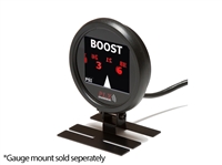
DM-200 OBD II
User Guide
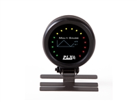
DM-6
User Guide

M-300 TE
User Guide

SM-AFR Combo
User Guide
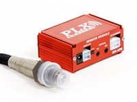
SM-AFR
User Guide
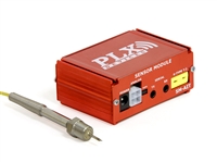
SM-AIT
User Guide
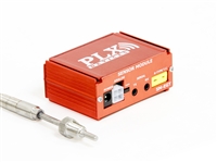
SM-EGT
User Guide
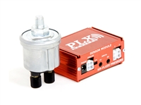
SM-FP
User Guide
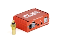
SM-FT
User Guide

SM-V/B
User Guide

8V Converter
User Guide

SM-Pro
User Guide
Kiwi Car to Smartphone

Kiwi 3 User Guide
and Support

Kiwi 2 Bluetooth
User Guide

Kiwi 2 Wifi
User Guide
Luxor
Luxor LX735
User Guide
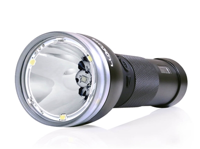
Luxor 2
User Guide

Luxor Mini
User Guide
KC1 Charger
User Guide
Legion Solar

Legion Solar
User Guide

Legion Solar
Electrical Connection Notes
Electronics

Legion 11000mAH (Gen2)
User Guide

Legion 5500mAh
User Guide

Legion Meter
User Guide
Retired Products

Kiwi MPG
User Guide

Kiwi Bluetooth
User Guide
Legion 11,000mAh (Gen1)
User Guide

Yaba Speaker
User Guide

Yaba X Speaker
User Guide
Software and Drivers
DM-100/200 Utility
DM-100/200 OBD II/Touch
Driver (32 bit OS)
DM-100/200 OBD II/Touch
Driver (64 bit OS)

R-Series
USB Driver

Custom Gauge
Library
Get on the list & get exclusive deals
Enter your email address for special offers from PLX Devices Inc.


© Copyright 2015, PLX Devices Inc. All Rights Reserved.